Research Highlights

Home \ Research \ Research Highlights

Phase matching in Vector-Beam Driven High Harmonic Generation in 3D-printed Gas Cells

December 1, 2025|

Laser driven x-ray sources are capable of achieving nanometer length scale imaging while simultaneously durations on the order of nanoseconds, enabling microscopy at the fastest timescales and the smallest length scales. Through the use of mid-infrared lasers, the generated light can extend into the soft x-ray regime, where there are exciting applications in biological imaging vvia the water window, magnetic imaging at the absorption edges of common magnetic materials, and scales appropriate for upcoming nodes of semiconductor lithography. Tabletop high harmonic sources (HHG) are a leading light source for this cutting edge microscopy, and is an area of expertise within STROBE. At the cutting edge, we are now capable of generating HHG with advanced polarizations, STROBE research has shown that HHG can generate x-rays with radial or azimuthal polarization.

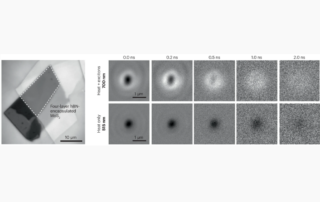
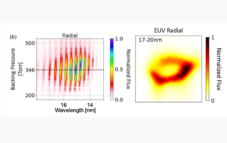
STROBE scientists have now combined both advanced polarization HHG with longer wavelength drivers, making soft x-ray vector polarization beams for the first time. Using specially designed 3D printed gas cells, they were able to make high brightness beams at 1300 nm driving wavelengths and measure the full pressure curve that describes the efficiency of generating light known as the phase matching curve. Even at harmonic orders surpassing the 71st was the ring like structure in the harmonic beam clearly observed, indicating high control over the driving wavelength and polarization. A model based on the laser modes and the imparted phase accurately predicted the change in pressure needed to efficiently generate light, expanding existing thery for use with these new vector polarization states.

Attiyah, H. Allison, J. To, P. Kazansky, D. Schmidt, C. Gardner, V. Flores, J. Lewis, C.G. Durfee, and F. Dollar, “Phase matching in Vector-Beam Driven High Harmonic Generation in 3D-printed Gas Cells,” Journal of the Optical Society of America B 42, 12 (2025). DOI: 10.1364/josab.572118

Multi-Element 3D Imaging with Soft X-ray Ptychography

September 18, 2025|

A new approach for high-resolution, three-dimensional elemental imaging has been demonstrated using soft X-ray ptychographic tomography. This technique leverages both optical density and phase contrast reconstructions to identify elements from a single-energy tilt series, reducing acquisition time by more than half compared to traditional multi-energy tomography. The method was validated on nickel-alumina catalyst particles, where nickel nanoparticles were distinguished from the porous alumina matrix with nanometer-scale resolution. By combining high optical density and low phase contrast signals near an absorption edge, nickel precipitates were identified robustly within the reconstructed volumes, providing critical insights into how metallic particles exsolve and redistribute under catalytic conditions.

This advance opens the door for efficient, element-specific 3D characterization of complex materials, with particular relevance for catalytic systems where nanoscale compositional changes drive performance. The approach not only streamlines experiments at synchrotron facilities, where acquisition time is highly limited, but also establishes a scalable framework for future studies involving multiple transition metals. Such capabilities are essential for unraveling the nanoscale dynamics of catalytic processes, and ultimately for guiding the design of more efficient and durable catalysts for environmentally important applications such as methane reforming.

J. PlumbA. DitterD. KimK. LeeY. YuD. Shapiro, "Multi-element tomography: leveraging absorption and phase contrast in soft X-ray ptychography" Proc. SPIE 13622-4, X-ray Nanoimaging: Instruments and Methods VII, (2025). DOI: 10.1117/12.3063920

Permanent magnet solenoid lenses for high brightness electron beams

August 20, 2025|

Researchers from SLAC and UCLA have developed a compact radially magnetized permanent-magnet solenoid (PMS) that brings high-performance focusing of relativistic electron beams into a form factor ideal for next-generation imaging tools. The dual-ring PMS generates axial magnetic fields up to 1 T and achieves focal lengths below 10 cm for relativistic electrons, offering a cost-effective power-free, cryogen-free alternative to conventional solenoids. Detailed field characterization and modeling confirmed its ability to deliver precise, axisymmetric focusing while minimizing aberrations, meeting the stringent requirements of modern electron imaging experiments.

Tests at UCLA’s Pegasus beamline showed that the PMS can reduce the transverse size of 7 MeV electron bunches by an order of magnitude, down to tens of microns, in excellent agreement with simulations. This capability unlocks new opportunities for high-resolution and high-speed imaging: in ultrafast electron diffraction, the PMS acts as a post sample lens to magnify reciprocal-space patterns beyond detector limits, while in inverse Compton sources or microprobes it enables sub-10 μm beam waists, boosting brightness and spatial resolution.

T. Xu, C. J. R. Duncan, P. Denham, B. H. Schaap, A. Kulkarni, D. Garcia, S. D. Anderson, P. Musumeci, and R. J. England. "Focusing of Relativistic Electron Beams With Permanent Magnetic Solenoid." Physical Review Accelerators and Beams 28.8 (2025). http://doi.org/10.1103/phhz-fgnl

An Exponential Convolutional Neural Network for Rapid Detection of Bacteria from Raman Spectra on Edge Devices

August 10, 2025|

The convolutional network is the preferred option for handling large input sizes and is commonly used in neural networks for most applications. In this experiment we demonstrate the performance of a modified convolutional neural networks (CNN) using an exponent based weight. The Exponential Convolutional Neural Network (ECNN) was tested on bacteria classification, with different model deployed on edge devices such as a Raspberry Pi and Esp32. Additionally, we created a model with 3-output that can detect a specific bacteria like E. coli, aiding environmental engineers in improving efficiency. As a result, our 4-layer standard CNN model was able to achieve an accuracy of 85% for 30 bacteria strains and this 4-layer model was successfully deployed to an edge device (the Raspberry Pi 5), with model quantization using TensorFlow Lite. ECNN is having an accuracy of 68% on test set and 89% accuracy training set. This study shows the potential of deploying a CNN for bacterial detection on edge devices. Future work will be focused on improving model generalization, reducing overfitting, and improving real-time inference performance to create a more reliable and efficient system for the environment and water quality monitoring.

This study demonstrates that CNNs can be deployed on edge devices for bacterial detection, highlighting the potential applications for environmental engineers. It offers a method for developing real-time, low-cost water quality monitoring systems. Future work will focus on refining the model architecture, addressing overfitting, and improving the overall reliability of bacterial detection on edge devices.

Kaifeng Liu, Wells Wait, and Yiyan Li. An Exponential Convolutional Neural Network for Rapid Detection of Bacteria from Raman Spectra on Edge Devices. IEEE MWSCAS 2025.

Point Defect Induced Potential Wells across the m-Plane of Core/Shell GaN Nanowires

August 5, 2025|

Semiconductor nanowires offer unique opportunities for next-generation electronic and photonic devices due to their high surface-to-volume ratio, ability to suppress dislocations, accommodate large lattice mismatches, and support both axial and radial heterostructure growth. In particular, the non-polar planes of GaN nanowires provide a promising platform for high-performance optoelectronics by mitigating quantum-confined Stark effects and reducing Auger recombination losses.

STROBE scientists, together with collaborators in Cambridge, Lund, and Denmark, report the discovery of unexpected electrostatic potential wells across the non-polar m-plane and at the core/shell interface in n-type GaN nanowires. Using off-axis electron holography (OAEH), quantum-well-like potential drops were mapped at both the core/shell interface and the nanowire center. Valance electron energy loss spectroscopy (VEELS) revealed localized bandgap narrowing of 30–40 meV in the same regions, while cathodoluminescence spectroscopy linked the reduced potential in the core to CN defects, and suggested VGaON defect complexes as the most likely origin of the non-radiative wells at the core/shell interface.

These findings demonstrate that point defects can play a dominant role in shaping electrostatic potential landscapes and optical properties of GaN nanowires. Since such defects act as non-radiative recombination centers, they have critical implications for the efficiency and design of nanowire-based LEDs, lasers, and quantum devices. The study highlights the need for careful defect management in epitaxial growth and provides a roadmap for understanding defect-driven electronic behavior in other III-V core/shell heterostructures.

S. Rezaie, G. Kusch, L. Samuelson, J.B. Wagner, S. Yazdi, "Point Defect Induced Potential Wells across the m-Plane of Core/Shell GaN Nanowires," Phys. Status Solidi RRL (2025). https://doi.org/10.1002/pssr.202500145

Ferroelectric electric field development with progressive annealing

July 25, 2025|

Ferroelectricity underpins many proposed next-generation memory technologies that are widely expected to have profound impacts on modern computing. Hf0.5Zr0.5O2 (HZO) is the leading material candidate for the ultimate commercial implementation of ferroelectric memory because it is CMOS compatible, it has a large spontaneous polarization, and it can retain its ferroelectric properties in films as thin as 1 nm. Unfortunately, the crystal phase of HZO responsible for its ferroelectricity (orthorhombic phase, space group number 29) competes with several other non-ferroelectric phases of similar free energies, making stabilization of the orthorhombic phase a challenge. Encapsulating electrodes seem to play an important role in stabilizing the ferroelectric phase, but the mechanism by which they do so remains poorly understood.

Here, we examine a ferroelectric HZO capacitor with titanium nitride (TiN) electrodes using scanning transmission electronmicroscopy (STEM) imaging in plan view. The capacitor is encircled by a lithographically-defined TiN heater that we energize in situ. Conventional STEM imaging identifies crystal grains in the TiN electrodes and in the HZO film. Simultaneously acquired STEM electron beam-induced current (EBIC) images provide electric field contrast that highlights the ferroelectric domains. At low annealing temperatures we find that the HZO’s ferroelectric domain structure is correlated with the TiN electrodes’ grain structure. Annealing at higher temperatures causes the domains to outgrow the TiN grains. Eventually the HZO domains expand to the size of the HZO grains they inhabit.

Royle, et al., “Limitations Imposed on Ferroelectric Domains in HZO by Electrode Grain Structure,” TECHCON 2025.   T. O'Neill, et al. “The Effect of Electrode Structure on Ferroelectric Domains in Hf0.5Zr0.5O2,” Microscopy & Microanalysis 31 (2025).

Ring deconvolution microscopy: exploiting symmetry for efficient spatially varying aberration correction

April 29, 2025|

The most ubiquitous form of aberration correction for microscopy is deconvolution; however, deconvolution relies on the assumption that the system’s point spread function is the same across the entire field of view. This assumption is often inadequate, but space-variant deblurring techniques generally require impractical amounts of calibration and computation. We present an imaging pipeline that leverages symmetry to provide simple and fast spatially varying deblurring. Our ring deconvolution microscopy method utilizes the rotational symmetry of most microscopes and cameras, and naturally extends to sheet deconvolution in the case of lateral symmetry. We derive theory and algorithms for ring deconvolution microscopy and propose a neural network based on Seidel aberration coefficients as a fast alternative. We demonstrate improvements in speed and image quality as compared to standard deconvolution and existing spatially varying deblurring across a diverse range of microscope modalities, including miniature microscopy, multicolor fluorescence microscopy, multimode fiber micro-endoscopy and light-sheet fluorescence microscopy. Our approach enables near-isotropic, subcellular resolution in each of these applications.

Kohli, A., Angelopoulos, A.N., McAllister, D. et al., “Ring deconvolution microscopy: exploiting symmetry for efficient spatially varying aberration correction,” Nature Methods 22, pages 1311–1320 (2025). http://doi.org/10.1038/s41592-025-02684-5

Interferometric scattering microscopy

April 10, 2025|

In many areas of non-invasive optical imaging, particularly in biology and materials science, the use of conventional fluorescence-based microscopy techniques is constrained by a number of factors, including the need for molecular labels and the occurrence of photobleaching. Optical scattering methods provide a powerful alternative that can overcome these limitations by detecting the inherent light-scattering properties of a sample. One such technique, interferometric scattering (iSCAT) microscopy, is a highly sensitive, label-free method that enables the detection of subwavelength entities, such as nanoparticles and single molecules, by using optical interference to translate a weak scattering signal into a strong, detectable intensity change. Because it is a label-free technique, it avoids issues like photobleaching and allows for the precise determination of a nanoparticle’s properties, such as size and mass. It is also highly effective for 3D tracking and quantifying ultrafast diffusion in solids.

STROBE contributed to an important review article in Nature Reviews Methods Primers that provides a comprehensive overview of iSCAT microscopy, its theoretical underpinning, practical implementation, and applications. In particular, STROBE’s contribution focuses on the Center’s development of stroboSCAT, an advanced, time-resolved variant of iSCAT. This innovative technique was created to address a critical challenge in materials science: the difficulty of quantitatively separating different physical phenomena, such as the generation of electronic charge carriers (excitons) and unwanted heat, which have overlapping optical signatures.

stroboSCAT employs a unique pump-probe and multi-wavelength strategy to quantitatively separate and map these contributions with exceptional spatiotemporal precision. This enables accurate observation and characterization of electronic, thermal, and mass transport in a wide range of materials at the nanoscale both separately and also in combination. This methodological advancement represents a significant step forward for fundamental research in optoelectronics and materials science, given the complexities of energy transport and conversion in next-generation functional materials.

For example, stroboSCAT is specifically applied to simultaneously map heat and exciton populations in materials like few-layer molybdenum disulfide (MoS₂). By enabling the quantitative separation of these signals, stroboSCAT transforms iSCAT from a general imaging platform into a powerful analytical instrument for resolving ultrafast energy transport and transduction at the nanoscale.

Ginsberg, N.S., Hsieh, C.-L., Kukura, P. et al., "Interferometric scattering microscopy." Nature Reviews Methods Primers 5, 1 (2025). DOI: 10.1038/s43586-025-00391-1.

Correlated nano-imaging of structure and dynamics of cation-polaron coupling in hybrid perovskites

February 26, 2025|

Triple cation perovskites (TCPs) are organic-inorganic hybrid materials that first rose to prominence as efficient photovoltaic materials, yet also hold promise for other applications like lasing, exciton condensation, single photon emitter, photodetectors, or photocatalysis. Their high performance continues to surprise considering the nano- and microscale heterogeneities and high defect densities of the typically polycrystalline thin films used. It is believed that the soft dynamically deformable lattice and mobile cations have the unique ability to stabilize charge carriers by polaron formation. However, the material science of perovskites has remained largely empirical with a lack of spectroscopic access to the elementary processes defined at the low-energy scale of the electron and lattice dynamics in the infrared. The relevant information with its inter- and intragrain heterogeneity in composition and structure is lost in conventional spatially averaged spectroscopy or static imaging. 

Here a STROBE team from CU Boulder in collaboration with researchers from imo-imomec (Belgium) combined three nano-imaging modalities developed through STROBE previously, and in the application to an important hybrid perovskite photovoltaic material, provide for the first time a real space view of composition, lattice structure, and carrier dynamics simultaneously. Mid-infrared nano-spectroscopy of the ground state vibrational response probing composition and the static lattice parameter was correlated with excited state spectroscopy resolving both ps- to ns- polaron relaxation and associated coupled lattice dynamics. The researchers could watch for the first time the transient lattice deformation and cation-lattice coupling as the polaron forms, grows, and evolves into the long-lived carriers giving rise to the photovoltaic response. Our work shows how correlated ground and excited state structural and dynamics nano-imaging could guide optimization of composition and thin film preparation to transform the field from the conventional trial and error approach to a targeted material design.

R. Wilcken, B. L. Esses, R. S. Nithyananda Kumar, L. A. Hurley, S. E. Shaheen, M. B. Raschke, "Correlated nanoimaging of structure and dynamics of cation-polaron coupling in hybrid perovskites," Science Advances, 11, eads3706, (2025). DOI: 10.1126/sciadv.ads3706

Dynamics and structure of the B2→ B19’phase transformation in NiTi revealed through in situ 4D-STEM

January 28, 2025|

Electron microscopy has been used throughout the years to visualize structural changes in materials undergoing phase transformations. However, there are always details about what happens right before a transformation and the repeatability of a transformation that are difficult to track. In this paper we demonstrated that electron microscopy coupled with high-speed direct electron detectors can be used to characterize the forward and reverse martensitic transformations exhibited in NiTi, with nanoscale precision, and at large fields of view. Our method enables direct observation and characterization of 3 unique B19′ martensite variants that are differentiated by the planes on which they appear. Moreover, we track their formation while cooling past the martensitic transformation temperature. The B19′ variant phases and associated strains are mapped at different temperature steps and are directly compared via intermittent 4D-STEM scans to study the transformation. The B2 austenite pre-transitional microstructure is compared to the martensite phase transformation after multiple temperature cycles in order to improve our understanding of cyclic evolution of the martensite lath structure. Our results demonstrated how 4D-STEM can improve our understanding of complex transformation mechanisms that are of particular importance for engineering materials such as shape memory alloys.

J Donohue, SH Mills, BH Savitsky, SE Zeltmann, C Ophus, AM Minor. “Dynamics and structure of the B2 B19'phase transformation in NiTi revealed through in situ 4D-STEM,” Materials Science and Engineering: A, 926, (2025), 147951. DOI: 10.1016/j.msea.2025.147951
Go to Top