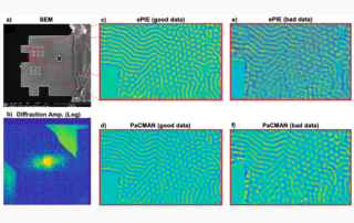
Computational microscopy with coherent diffractive imaging and ptychography
Microscopy and crystallography have long served as two foundational pillars of experimental science. Microscopy relies on lenses to visualize local structures, whereas crystallography determines the global atomic arrangement of crystals through diffraction. Over the past two decades, these traditionally distinct methodologies have been unified through the rise of computational microscopy, particularly coherent diffractive imaging (CDI) and ptychography. These approaches replace physical lenses with coherent scattering and algorithmic phase retrieval, overcoming long-standing resolution limits in conventional imaging. In a recent comprehensive review, Miao summarized how CDI and ptychography now deliver exceptional imaging performance across nine orders of magnitude in length scale, from sub-angstrom visualization of atomic structures to quantitative phase imaging of centimeter-scale tissues, all based on the same underlying physical principles and closely related iterative algorithms.
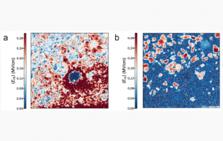
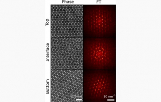
Beyond 2D reconstruction, CDI and ptychography can be integrated with advanced tomographic methods to achieve 3D imaging with unprecedented detail. These combined techniques have enabled the 3D atomic structure determination of crystal defects and amorphous materials, the mapping of magnetic and electronic textures in quantum and energy materials, and high-resolution, non-destructive 3D characterization of nanomaterials and integrated circuits. They have also facilitated quantitative phase imaging of biological tissues, cells, viruses, and protein complexes, extending computational microscopy into the life sciences.
The rapid progress in this field is driven by the convergence of multiple technological advances, including fourth-generation synchrotron radiation sources, X-ray free-electron lasers, tabletop high-harmonic generation, state-of-the-art electron and optical microscopes, high-dynamic-range detectors, and deep-learning–accelerated phase retrieval. As these capabilities continue to evolve, CDI and ptychography are poised to make even broader and deeper contributions across physics, chemistry, materials science, engineering, biology, and medicine in the coming years.