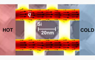
Two-color high-harmonic generation from relativistic plasma mirrors
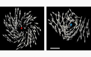
Circularly polarized x-rays have a number of microscopy applications that leverage the rotational nature of some physical systems, one of the most common applications being magnetic dichroism of nanoscale magnetic devices. Generating circularly polarized x-rays, particularly coherent x-rays with ultrafast pulse durations is practically difficult and inefficient. One of the major successes of STROBE was the development of not just one, but two mechanisms for generating circularly polarized x-rays using light at moderate intensities in the strong field regime. In this work, we lay the foundation for scaling analogous mechanisms into the relativistic regime. In this regime, the energy cutoff can be much higher than in the strong field. Performing numerical simulations, we confirm that despite the physical mechanism being completely different at relativistic intensities, the same conservation laws observed in the earlier STROBE work are still valid in the relativistic regime. Experiments are being planned to demonstrate this mechanism in the lab, which can leverage new facilities such as the NSF ZEUS which would enable high single shot flux in dichroism experiments.