Reduced-Dimensionality Al Nanocrystals: Nanowires, Nanobars, and Nanomoustaches
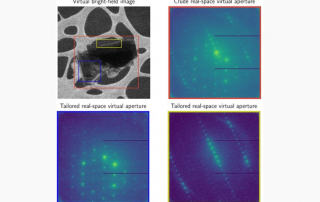
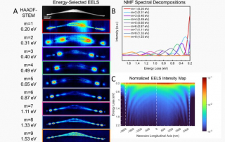
Aluminum nanocrystals created by catalyst-driven colloidal synthesis support excellent plasmonic properties, due to their high level of elemental purity, monocrystallinity, and controlled size and shape. Reduction in the rate of nanocrystal growth enables the synthesis of highly anisotropic Al nanowires, nanobars, and singly twinned “nanomoustaches”. Electron energy loss spectroscopy was used to study the plasmonic properties of these nanocrystals, spanning the broad energy range needed to map their plasmonic modes. The coupling between these nanocrystals and other plasmonic metal nanostructures, specifically Ag nanocubes and Au films of controlled nanoscale thickness, was investigated. Al nanocrystals show excellent long-term stability under atmospheric conditions, providing a practical alternative to coinage metal-based nanowires in assembled nanoscale devices.