masonlw

Home \ Lauren Mason

About Lauren Mason

This author has not yet filled in any details.
So far Lauren Mason has created 274 blog entries.

CU Students Become Solar Scientists

An unusual research project at the University of Colorado turned more than a thousand undergrad students into instant solar scientists.

X-Ray/Raman Microfluidics Postdoctoral Fellow

Join our team at Lawrence Berkeley National Lab’s (LBNL) Chemical Sciences (CSD) Division as a Postdoctoral Scholar in developing X-Ray and vibrational spectroscopy techniques coupled to microfluidics. 

In this role, you will contribute to the development of a multimodal-in situ experimental platform for controlling the latent heat in phase change materials (PCMs) for thermal energy storage. You will leverage the potential of metal organic compounds with hydrogen and coordination bonds to modulate phase transition through inter and intramolecular interactions. By employing an advanced, multimodal characterization platform, that includes  in situ/multimodal Raman spectroscopy, X-ray scattering, ambient pressure X-ray photoelectron spectroscopy & synchrotron based Infrared Nano-spectroscopy at the Advanced Light Source, your work will provide molecular-level mechanistic insights into PCMs across various length and time scales.

Read more and apply here: https://jobs.lbl.gov/jobs/x-ray-raman-microfluidics-postdoctoral-fellow-5878

Margaret Murnane is Awarded a Honorary Doctorate from the University of Salamanca

Renowned scientist, JILA Fellow, and University of Colorado Boulder professor Margaret Murnane has been granted an honorary doctorate from the prestigious University of Salamanca, recognizing her outstanding contributions to the field of ultrafast laser science. As a trailblazer in her field, Murnane’s groundbreaking research has revolutionized our understanding of light and opened up new avenues for scientific discovery and technological innovation. This esteemed recognition from one of the oldest universities in the world serves as a testament to Murnane’s remarkable achievements and lasting impact on the scientific community.

Turning Up the Heat in Quantum Materials

Quantum materials, a fascinating class of materials that harness the power of quantum mechanics, are revolutionizing modern science and technology. Quantum materials often possess exotic states of matter, such as superconductivity or magnetic ordering, that defy conventional understanding and can be manipulated for various technological applications. To further enhance and manipulate the intriguing characteristics of quantum materials, researchers leverage nanostructuring—the ability to precisely control the geometry on the atomic scale. Specifically, nanostructuring provides the ability to manipulate and fine-tune the electrical and thermal properties of quantum and other materials. This can result, for example, in designer structures that conduct current very well, but impede heat transport. These structures can help recapture and utilize waste heat in electronics, buildings, and vehicles—enhancing their efficiency and, thereby, reducing power consumption. A related critical challenge for a broad range of nanotechnologies is the need for more efficient cooling, so that the nano devices do not overheat during operation. To better understand heat transport at the nanoscale, JILA Fellows Margaret Murnane, Henry Kapteyn, and their research groups within the STROBE NSF Center, JILA and the University of Colorado Boulder, created the first general analytical theory of nanoscale-confined heat transport, that can be used to engineer heat transport in 3D nanosystems—such as nanowires and nanomeshes—that are of great interest for next-generation energy-efficient devices. This discovery was published in NanoLetters. 

Congratulations to Nathan Brooks on a Postdoctoral Fellowship, Academia Sinica, Taiwan

Congratulations to Nathan Brooks for receiving a Postdoctoral Fellowship from Academia Sinica in Taiwan!

Semiconductor Metrology Applications Engineer

JOB DESCRIPTION 

We are seeking a highly motivated scientist or engineer to join our team and support business growth with semiconductor customers in the United States. The Applications Engineer will work closely with customers and be responsible for translating customer issues into problem statements for UNISERS.  The Applications engineer will represent UNISERS as a technical expert in the field and establish recognition of this expertise from the customer. The scope and impact of this role offers the opportunity to grow in technical expertise or project or management leadership positions.

RESPONSIBILITIES & TASKS 

  • Coordinating and executing activities with our customers, understanding their needs, and delivering customized solutions.
  • Conducting experiments and developing applications with customers to secure new business.
  • Providing local expertise for maintenance, troubleshooting, and repairs of UNISERS equipment at our customer sites.
  • Managing customer expectations by aligning goals and making expectations clear to others.
  • Securing confidentiality of customer data, while translating customer issues into problem statements for UNISERS.
  • Collaborating with multi-functional teams to support new technology development and accelerate product commercialization.
  • Challenging the status quo to strive for improvements that add value.
  • Keeping up to date with the latest trends and developments in small particle detection and identification.
  • Communicating effectively with customers and internal teams through written and oral presentations.

SKILLS & EXPERIENCE 

  • Master’s degree or 2 years working experience in Material Science, Chemistry, Physics, Engineering, or a related field
  • Broad and deep experience with all kinds of analytical methods for nanoparticles and surfaces.
  • Experience with semiconductor-grade high-purity material testing and validation.
  • Experience with application development for semiconductor R&D or manufacturing.
  • Intermediate programing experience in Python is preferred.
  • Excellent written and oral presentation skills.
  • Fluency in English and German is advantageous.

PERSONAL CHARACTERISTICS 

  • Fast learner with a strong self-motivation to grow technically.
  • Willingness to be cross trained in both applications development and equipment maintenance.
  • Strong problem-solving skills; ability to work through ambiguity, in a dynamic environment.
  • A high level of integrity for securing customer confidentiality.
  • Ability to work independently and follow through on assignments with minimal supervision.
  • Respecting each other and embracing the diversity of working in a cross-cultural team.
  • Caring for our environment and avoiding waste.
  • Willing to travel within the US to customers and to Switzerland for trainings.

ABOUT UNISERS 

UNISERS AG is a young start-up from ETH Zurich with revolutionary technology to tackle the biggest challenge in the semiconductor industry: namely, contamination control. Our patented products have been validated to tremendously help the whole semiconductor supply chain (components, materials, wafers, equipment, and chip fabs) with quality control by finding and identifying otherwise undetected or unknown contaminations. Therefore, we will help chip makers reduce the amount of wasted chips (often more than 50%), increasing their profit substantially and at the same time contributing to less waste and CO2 emissions. Having closed a 14 Mio $ seed investment round led by Intel Capital; we are scaling up our team to bring our unique technology to industry as fast as possible.

BENEFITS 

  • Competitive salary and benefit packages (including health insurance, dental insurance, vision insurance, life insurance and 401K matching)
  • Participation in our attractive ESOP (Employee Stock Option Plan)
  • Opportunity to shape a growing high-tech company and take over leadership roles
  • Modern culture of collaboration
  • 25 days of vacation
  • Flexible working hours, including possibility for remote work
  • Personal education (reimbursement of tuition fees)

How hundreds of college students are helping solve a centuries-old mystery about the sun

Astronomers-in-training spent thousands of hours peering at tiny solar flares that space telescopes missed. A team of more than 1,000 astronomers and college students just took a step closer to solving one of the long-lasting mysteries of astronomy: Why is the sun’s outer layer, known as the corona, so ridiculously hot? The solar surface is 10,000°F, but a thousand miles up, the sun’s corona flares hundreds of times hotter. It’s like walking across the room to escape an overzealous space heater, but you feel warmer far away from the source instead of cooler, totally contrary to expectations.

Predicting heat flow in 3D semiconductor nanosystems

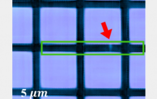
Nanostructuring on length scales corresponding to phonon mean free paths provides control over heat flow in semiconductors and makes it possible, in principle, to engineer their thermal properties. However, this is currently not feasible because there is no general description for heat flow in 3D nanostructured semiconductors. In recent research, STROBE scientists used short wavelength extreme ultraviolet beams to study heat transport in a silicon metalattice with deep nanoscale features. They observed dramatically reduced thermal conductivity relative to bulk—about x50 times less than current model predictions. To explain this, they developed a new predictive theory that incorporates the idea that heat-carrying lattice vibrations can behave like a fluid—spreading out instead of just moving ballistically in straight lines. Moreover, this new theory of heat transport can be used to predict and engineer phonon transport in many other 3D nanosystems including nanowires and nanomeshes, that are of great interest for next-generation energy-efficient devices.

How 1,000 undergraduates helped solve an enduring mystery about the sun

For a new study, a team of physicists recruited roughly 1,000 undergraduate students at CU Boulder to help answer one of the most enduring questions about the sun: How does the star’s outermost atmosphere, or “corona,” get so hot? The research represents a nearly-unprecedented feat of data analysis: From 2020 to 2022, the small army of mostly first- and second-year students examined the physics of more than 600 real solar flares—gigantic eruptions of energy from the sun’s roiling corona…

Introduction to Electron Microscopy for Materials Science

Abstract: This talk will introduce the basics of Transmission Electron Microscopy (TEM)  imaging, spectroscopy and diffraction techniques to a general audience and show recent highlights of new techniques for materials characterization. Modern TEMs combine atomic-level imaging and spectroscopy with quantitative diffraction analysis, providing a powerful toolkit for probing the structure and chemistry of materials. Recent technological advances in instrumentation such as stages and direct electron detectors have enabled new capabilities and modes of imaging.  This talk will also highlight selected in situ observations of the dynamic physical behavior of materials in response to external stimuli such as temperature, environment, stress, and applied fields.

Bio: Andrew Murphy Minor is a Professor at the University of California, Berkeley in the Department of Materials Science and Engineering and also holds a joint appointment at the Lawrence Berkeley National Laboratory where he is the Facility Director of the National Center for Electron Microscopy in the Molecular Foundry. He has over 260 publications in the fields of nanomechanics, metallurgy, electron characterization of soft matter and in situ transmission electron microscopy technique development. Minor’s honors include the LBL Materials Science Division Outstanding Performance Award (2006 & 2010), the AIME Robert Lansing Hardy Award from TMS (2012) and the Burton Medal from the Microscopy Society of America (2015). Currently, he is the President of the Microscopy Society of America.

Go to Top