masonlw

Home \ Lauren Mason

About Lauren Mason

This author has not yet filled in any details.
So far Lauren Mason has created 237 blog entries.

Tutorial: Introduction to Computational Imaging

Abstract: This tutorial will introduce computational imaging as a broad range of techniques in which algorithms play a major role in the final image formation process. The basic recipe for computational imaging involves coming up with a forward model that can simulate/predict what your imaging system measures. This model is computationally inverted to reconstruct the object under investigation. We will also discuss how to incorporate prior knowledge and constructs from machine learning into the computational reconstruction algorithms to improve the image reconstruction fidelity. The tutorial will include examples from computational optical imaging, such as diffusercam and diffraction tomography.
Bio: Kevin C. Zhou is a postdoctoral researcher at UC Berkeley, working with Profs. Laura Waller and Hillel Adesnik. His research is centered around developing high-throughput, data-intensive computational 3D imaging systems for a broad range of applications, with interests spanning optical coherence tomography, diffraction tomography, lidar, ptychography, nonlinear microscopy, and parallelized 3D microscopy. Kevin is a recipient of the Barry M. Goldwater Scholarship, the NSF Graduate Research Fellowship, and the Schmidt Science Fellowship.

Shades of Gray: Scientific Integrity and Research Misconduct

Title: Shades of Gray: Scientific Integrity and Research Misconduct
Presenter: Prof. Markus Raschke, Professor, Physics and JILA, University of Colorado Boulder, STROBE Director of Knowledge Transfer
Abstract: Research misconduct refers to the fabrication, falsification, or plagiarism in proposing, performing, or reviewing research or in reporting research results. However, the situation is often much less clear than these formal definitions may imply. I will discuss the background and go over a range of case studies based on over 20 years of work in different ombuds and committee roles on this subject. We will discuss distinction from research error and everything in between from questionable research practices to outright misconduct. While the general rules are clear, many challenges abound in identifying, investigating, and prosecuting research misconduct. With limited resources and multi-level conflicts of interest between perpetrators, supervisors, institutions, journals, and sponsors, best practices and procedure are still poorly implemented at many institutions. I will discuss from the many shades of gray of the subject to new rules of data and record keeping.
Speaker Bio: Markus Raschke is professor at the Department of Physics and JILA at the University of Colorado at Boulder. His research is on the development and application of nano-scale nonlinear and ultrafast spectroscopy to control the light-matter interaction on the nanoscale. These techniques allow for imaging structure and dynamics of molecular and quantum matter with nanometer spatial resolution. He received his PhD in 2000 from the Max-Planck Institute of Quantum Optics and the Technical University in Munich, Germany. Following research appointments at the University of California at Berkeley, and the Max-Born-Institute in Berlin, he became faculty member at the University of Washington in 2006, before moving to Boulder in 2010. He is fellow of the Optical Society of America, the American Physical Society, the American Association for the Advancement of Science, and the Explorers Club.

“From 3D to 2D and back again” (Prof. Psaltis) and “Volumetric printing in scattering resins” (Prof. Christophe Moser)

Title: From 3D to 2D and back again
Presenter: Prof. Demetri Psaltis, Professor of Optics and the Director of the Optics Laboratory at the Ecole Polytechnique Federale de Lausanne (EPFL)
Abstract: The prospect of massive parallelism of optics enabling fast and low energy cost operations is attracting interest for novel photonic circuits where 3-dimensional (3D) implementations have a high potential for scalability. Since the technology for data input–output channels is 2-dimensional (2D), there is an unavoidable need to take 2D-nD transformations into account. Similarly, the 3D-2D and its reverse transformations are also tackled in a variety of fields such as optical tomography, additive manufacturing, and 3D optical memories. Here, we review how these 3D-2D transformations are tackled using iterative techniques and neural networks. This high-level comparison across different, yet related fields could yield a useful perspective for 3D optical design.
Title: Volumetric printing in scattering resins
Presenter: Prof. Christophe Moser, Director of the MicroEngineering Section at the Ecole Polytechnique Federale de Lausanne (EPFL)
Abstract: 3D printing has revolutionized the manufacturing of volumetric components and structures in many areas. Several fully volumetric light-based techniques have been recently developed thanks to the advent of photocurable resins, reaching print time of few tens of seconds while keeping sub 100 um resolution. We will review a variety of materials that have been reported by several groups including ours and that includes soft cell loaded hydrogels, acrylates, glass, ceramics that have been printed with volumetric printing.  However, these new approaches only work with homogeneous and relatively transparent resins.

We will show a method that considers light scattering in the resin prior to computing projection patterns. Using a tomographic volumetric printer, we experimentally demonstrate that implementation of this correction is critical when printing objects whose size exceeds the scattering mean free path.

The Swirling Spins of Hedgehogs

Though microscopes have been in use for centuries, there is still much that we cannot see at the smallest length scales. Current microscopies range from the simple optical microscopes used in high school science classes, to x-ray microscopes that can image through visibly-opaque objects, to electron microscopes that use electrons instead of light to capture images of vaccines and viruses. However, there is a great need to see beyond the static structure of an object—to be able capture how a nano- or biosystem functions in real time, or to visualize magnetic fields on nanometer scales. A team of researchers from the STROBE Center have been working together to overcome these challenges. STROBE is an NSF Science and Technology Center that is building the microscopes of tomorrow. A large multidisciplinary team from the Miao and Osher groups from UCLA, the Kapteyn-Murnane group at CU Boulder, Ezio Iacocca from CU Colorado Springs, David Shapiro and collaborators at Lawrence Berkley National Laboratory, and the Badding and Crespi groups from Pennsylvania State University. They developed and implemented a new method to use x-ray beams to capture the 3D magnetic texture in a material with very high 10-nanometer spatial resolution for the first time (published in Nature Nanotechnology, see reference below).

Hedgehogs and Anti-Hedgehogs

The team investigated a nanostructured magnetic sample, consisting of tiny spheres of nickel, only ~30nm across, connected together by slender few-nm “necks” of nickel, that together form a structure called a magnetic metalattice. This complex nanostructured magnet is expected to produce swirling magnetic fields with topological spin textures that are far more complex than in a uniform magnet. These are called 3D topological magnetic monopoles – or hedgehogs, due to their spiny shape in magnetic rotation – if the magnetic field points outward. Conversely, they can be thought of anti-hedgehogs if the magnetic field points inward.  However, until recently, there was no experimental method to measure the 3D spin texture at the deep nanoscale. Using advanced algorithms to recover the image, and a microscope at the x-ray synchrotron light source at the Lawrence Berkley National Laboratory, the researchers overcame these challenges.

Imaging spin textures is extremely important, as it can help physicists to better understand magnetism at a fundamental level, and to design more energy-efficient data storage, memory, and nanodevices.  Using electron microscopy, one can capture beautiful 2D images of a static spin-texture, but it is challenging to capture a full 3D image. In the past, other scientists were able to capture a 3D image at a spatial resolution of about 100 nanometers, but they had to make assumptions about the sample to extract the 3D image. With this new technique, researchers do not have to make any assumptions.

Armed with this new visualization technique, the team of researchers is excited to study spin textures further. STROBE is developing tabletop setups and helping with national facilities that can capture the static and dynamic spin texture in materials. All algorithms developed for this data analysis will be open-sourced soon. In this experiment, as with others, they found that collaboration is key for moving scientific progress forward.

Humans of JILA: Brendan McBennett

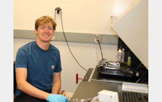
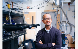
Surrounded by some of the world’s most advanced lasers, computers, and microscopes sits Brendan McBennett, a graduate student at JILA. McBennett has been working in the laboratories of JILA Fellows Margaret Murnane and Henry Kapteyn, as part of the KM group since 2019, excited to see his research advance significantly over that time. “We use ultraviolet and extreme ultraviolet (EUV) lasers to study heat flow in nanostructured materials,” McBennett states. “EUV photons have a higher photon energy that makes them insensitive to electron dynamics in most materials, combined with nanometer wavelengths. This allows them to very precisely probe surface deformations induced by heat – or thermal phonons – to capture new materials behaviors.”

Congratulations to Brendan McBennett for Being Named as the 2023 Recipient of the Nick Cobb Memorial Scholarship

Brendan McBennett has been announced as the 2023 recipient of the $10,000 Nick Cobb Memorial Scholarship by SPIE, the international society for optics and photonics, and Siemens EDA — formerly Mentor, a Siemens company — for his potential contributions to the field related to advanced lithography. McBennett will also be honored during 2023’s SPIE Advanced Lithography + Patterning conference.

The Nick Cobb scholarship recognizes an exemplary graduate student working in the field of lithography for semiconductor manufacturing. The award honors the memory of Nick Cobb, who was an SPIE Senior Member and chief engineer at Mentor. His groundbreaking contributions enabled optical and process proximity correction for IC manufacturing. Originally funded for three years ending in 2021, the Nick Cobb scholarship will be awarded to one student annually for an additional period of three years, through 2024.

Congratulations to Chen-Ting Liao for Receiving a Young Investigator Research Program Award from the Air Force Office of Scientific Research

Dr. Chen-Ting (Ting) Liao has been selected as an AFOSR Young Investigator. The Air Force Office of Scientific Research, or AFOSR, the basic research arm of the Air Force Research Laboratory, will award approximately $25 million in grants to 58 scientists and engineers from 44 research institutions and businesses in 22 states under the fiscal year 2023 Young Investigator Research Program, or YIP.

“Through the YIP, the Department of the Air Force fosters creative basic research in science and engineering, enhances early career development of outstanding young investigators and increases opportunities for the young investigators to engage in forwarding the DAF mission and related challenges in science and engineering,” said Ellen Robinson, YIP program manager.

YIP recipients receive three-year grants of up to $450,000. The program is open to U.S. citizens and permanent residents who are scientists and engineers at U.S. research institutions. Individuals must have received Ph.D. or equivalent degrees in the last seven years and show exceptional ability and promise for conducting basic research of Department of the Air Force, or DAF, relevance. Award selections are subject to successful completion of negotiations with the academic institutions and businesses.

Simultaneous Successive Twinning Captured by Atomic Electron Tomography

Shape-controlled synthesis of multiply twinned nanostructures is an important area of study in nanoscience, motivated by
the desire to control the size, shape, and terminating facets of metal
nanoparticles for applications in catalysis and other technologies. Controlling both the size
and shape of solution-grown nanoparticles relies on an understanding
of how synthetic parameters alter nanoparticle structures during
synthesis. However, while nanoparticle populations at the end of synthesis can be studied with standard electron microscopy methods, transient
structures that appear during some synthetic routes are difficult to observe. This is because these structures are often polycrystalline, with complicated overlapping crystal grains when that are difficult to interpret from a two-dimensional image.

A STROBE team from UC Berkeley and LBNL collaborated to study the
prevalence of transient structures during growth of multiply twinned
particles while also employing atomic electron tomography to reveal the atomic-scale three-dimensional structure of a Pd nanoparticle undergoing a shape transition, from decahedron to icosahedron. By identifying over 20,000 atoms within the structure, then classifying them according to their local crystallographic environment, we observe a multiply twinned structure consistent with a simultaneous successive twinning from a decahedral to icosahedral structure.

Imaging the electron wind force

Electromigration is one of the most critical problems limiting the future scaling of integrated circuits (ICs).  As more transistors are packed into ever smaller volumes, the total length of interconnecting wire is increasing as the wire simultaneously becomes narrower and more vulnerable to failure. Surprisingly, while chip fabs are presently churning out microprocessors at the “5-nm process node” with correspondingly tiny interconnects, before recent work by a STROBE team no measurements of electromigration pressures had been reported at length scales smaller than 10 μm.

Using electron-beam lithography, the  team fabricates tiny aluminum nanowires on electron-transparent silicon nitride membranes. They then apply an electrical current density of 108 A/cm2,  which is enough to drive electromigration, and map the nanowire’s density with parts-per-thousand precision using electron energy loss spectroscopy (EELS) in a scanning transmission electron microscope (STEM).  Two separable effects appear.  First, thermal expansion decreases the wire’s density as Joule heating raises its temperature. Using aluminum’s known coefficient of thermal expansion, one can convert the density map into a temperature map with the same spatial resolution.  Second, via the electron “wind force” the electrical current simultaneously compresses one end of the wire while it tensions the other. Using aluminum’s known bulk modulus,  one can convert the density map into a pressure map.  The temperature effect is independent of the direction of the current, while the pressure effect changes sign with the current’s direction, which allows the two effects to be separated.  Thus the thermodynamic state variables T and P can be mapped with high spatial resolution everywhere inside the wire. The ability to simultaneously see the prompt thermal and electron-wind-force effects in nanoscale interconnects opens entirely new avenues for studying electromigration, a key technological problem in the microprocessors powering modern computing devices.

Nano-imaging functional materials at their elementary scale

Any realistic operation of quantum technologies will require counteracting the effects of dissipation and dephasing. In particular, the wide range of photovoltaic, molecular electronic, or novel semiconductors are subject to many coupled internal degrees of freedom, structural heterogeneities, and coupling to the environment leading to the premature loss from conduction carriers to quantum information. Understanding and ultimately controlling the coupled quantum dynamics requires imaging the elementary excitations on their natural time and length scales. To achieve this goal, STROBE developed a new scanning probe microscope with ultrafast and shaped laser pulse excitation for multiscale spatial, spectral, and temporal optical nano-imaging. In this work the researchers developed heterodyne visible-pump IR-probe nano-imaging with far from equilibrium excitation to selectively probe excited state dynamics related to material function. In corresponding ultrafast movies, the fundamental quantum dynamics down to the few-femtosecond regime with nanometer spatial resolution can be resolved. This allowed to visualize in space and time competing electron and phononic processes in the application to solar-cell relevant polaron dynamics in perovskites as well as the insulator-to-metal transition in a correlated quantum material. Resolving these elementary processes related to the performance of these and other functional materials provides a perspective for the future targeted design of optimized and novel photonic and electronic material systems.

Go to Top