Tip-enhanced imaging and control of infrared strong light-matter interaction
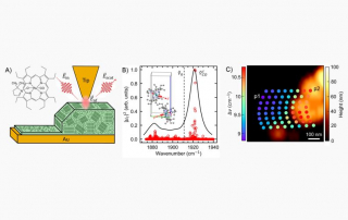
Strong coupling refers to the coherent interaction between quantum state transitions and optical modes. These hybrid states present new possibilities for applications such as single-molecule sensing, single photon emitters, and low-threshold solid state lasers. However, due to the fundamental limitation arising from the weak transition dipole moments in the infrared (IR), reaching the strong coupling regime has been limited to macroscopic ensembles. Recently, multi-quantum-wells (MQW) with quantum engineered electronic states offer a promising route towards mid-IR electronic strong coupling. However, with traditional diffraction-limited mode volumes, even for high Q-factor resonators, the strong coupling of a single quantum emitter has historically necessitated operation at cryogenic temperatures to counteract dissipation.
Here, a STROBE team from CU Boulder with collaborators from Sandia National Lab, the Walter Schottky Institute (Munich), Texas A&M, and Colgate University, achieved control of nonlinear IR light-matter interaction between a single nano-antenna and quantum well intersubband transitions. The team combined broadband synchrotron infrared nano-spectroscopy (SINS) at the ALS-LBL with intense fs/ps-pulsed IR s-SNOM imaging developed at CU Boulder for the dynamic manipulation of the antenna-quantum well hybrid states on the nanoscale. The results demonstrate the potential for localized and dynamic modification of quantum states and excitation pathways as a new regime of coherent and tunable IR electronic strong coupling in open nano-cavity systems, with the perspective of nano-scale sensing and nano-optical control of power limiters or saturable absorbers.