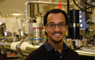
masonlw

Home \ Lauren Mason

About Lauren Mason

This author has not yet filled in any details.
So far Lauren Mason has created 240 blog entries.

STROBE Seminar: Patent Law and Intellectual Property

This seminar will include a brief discussion of patents and patent law including the purposes of patents (such as licensing, assets of a company, something to put on your resume), how they are structured (and how they are different from scientific papers), and careers in the patent law field.

About the speaker: Jennifer Bales has a BS in engineering from California State University Northridge and an MS in electrical engineering, specializing in optics, from University of Southern California.  Before going to law school at the University of Colorado, she worked in aerospace in the fields of ECCM, infrared image processing, and synthetic aperture radar (SAR) ground stations.  Her current patent work emphasizes optics, image processing, and signal processing, along with thermodynamics (in the area of refrigeration and air conditioning), medical devices, and various other electrical and mechanical inventions. She has been working as a patent attorney for over twenty years and has helped clients attain over 100 patents.

Cool it: Nano-scale discovery could help prevent overheating in electronics

A team of physicists and engineers at CU Boulder have solved the mystery behind a perplexing phenomenon in the nano realm: why some ultra-small heat sources cool down faster if you pack them closer together. The research began with an unexplained observation: a team led by Margaret Murnane and Henry Kapteyn at JILA were experimenting with metallic nanolines on a silicon substrate that when heated with a laser, something strange occurred. Nanoscale heat sources do not usually dissipate heat efficiently. But if you pack them close together, they cool down much more quickly.

Now, the researchers know why it happens. The team joined forces with a group of theorists led by Mahmoud Hussein in Aerospace Engineering Sciences to use computer-based simulations to track the passage of heat from their nano-sized bars. The simulations were so detailed that they could follow the behavior of each and every atom in the model—millions of them in all. They discovered that when they placed the heat sources close together, the vibrations of energy (called phonons) they produced bounced off each other more efficiently when other heat sources were nearby, scattering heat away and cooling the bars down.

The group’s results highlight a major challenge in designing the next generation of tiny devices, such as microprocessors or quantum computer chips. When you shrink down to very small scales, heat does not always behave the way you think it should.

Seeing with the “Nano” Eye

Understanding the chemical and physical properties of surfaces at the molecular level has become increasingly relevant in the fields of medicine, semiconductors, rechargeable batteries, etc. For example, when developing new medications, determining the chemical properties of a pill’s coating can help to better control how the pill is digested or dissolved. In semiconductors, precise atomic level control of interfaces determines performance of computer chips. And in batteries, capacity and lifetime is often limited by electrode surface degradation.  These are just three examples of the many applications in which the understanding of surface coatings and molecular interactions are important.

The imaging of molecular surfaces has long been a complicated process within the field of physics. The images are often fuzzy, with limited spatial resolution, and researchers may not be able to distinguish different types of molecules, let alone how the molecules interact with each other. But it is precisely this–molecular interactions–which control the function and performance of molecular materials and surfaces.  In a new paper published in Nano Letters, JILA Fellow Markus Raschke and graduate student Thomas Gray describe how they developed a way to image and visualize how surface molecules couple and interact with quantum precision. The team believes that their nanospectroscopy method could be used for molecular engineering to develop better molecular surfaces, with controlled properties for molecular electronic, photonic, or biomedical applications.

Congratulations to Mary Scott for Being named the Ted Van Duzer Endowed Professor in the UC Berkeley Department of Materials Science & Engineering

Congratulations to Mary Scott for Being named the Ted Van Duzer Endowed Professor in the UC Berkeley Department of Materials Science & Engineering. This professorship supports the work of a “promising non-tenured Professor in the College of Engineering”. The award also comes with financial support for Professor Scott’s research and students. The professor is named for Professor Ted Van Duzer, who is currently a Professor Emeritus in the Department of Electrical Engineering and Computer Sciences at Berkeley. Congratulations to Professor Scott for this wonderful and highly-deserved honor.

Tutorial: Electron Microscopy: Introduction, Applications and Opportunities

Electron microscopy is a high-resolution suite of characterization techniques used in the physical and biological sciences. By accelerating electrons to relativistic speeds (i.e. 0.5c) such that their characteristic wavelengths are 100,000 times smaller than visible light, one can perform high-resolution imaging down to the atomic scale. Furthermore, by implementing an array of diffraction and spectroscopic methods, electron microscopy can be used to decipher the nanoscale structure and composition of materials. This tutorial will begin by introducing electron microscopy and highlighting its advantages and disadvantages over visible and x-ray characterization techniques. Following this, the applications of electron microscopy will be summarized, with a specific focus on the cutting-edge experiments being performed by members of the STROBE community.

Congratulations to Naomi Ginsberg for being elected as a 2021 APS Fellow

Congratulations to Naomi Ginsberg for being named a the innovative development of spatiotemporally resolved imaging and spectroscopy methods, and for their use in elucidating energy transport in hierarchical and heterogeneous materials, as well as in the formation and transformation of said materials.

The APS Fellowship Program was created to recognize members who may have made advances in physics through original research and publication, or made significant innovative contributions in the application of physics to science and technology. They may also have made significant contributions to the teaching of physics or service and participation in the activities of the Society.

Fellowship is a distinct honor signifying recognition by one’s professional peers. Each year, no more than one half of one percent of the Society’s membership (excluding student members) is recognized by their peers for election to the status of Fellow of the American Physical Society.

Three-dimensional atomic packing in amorphous solids with liquid-like structure

Liquids and solids are two fundamental states of matter. Although the structure of crystalline solids has long been solved by crystallography, our understanding of the 3D atomic structure of liquids and amorphous materials remained speculative due to the lack of direct experimental determination. Now, a collaborative team from UCLA, Lawrence Berkeley National Lab and Brown University has advanced atomic electron tomography to determine for the first time the 3D atomic positions in monatomic amorphous materials, including a Ta thin film and two Pd nanoparticles. Despite different chemical composition and synthesis methods, they observed that pentagonal bipyramids are the most abundant atomic motifs in these amorphous materials. Contrary to traditional understanding, most pentagonal bipyramids do not assemble icosahedra, but are closely connected to form networks extending to medium-range scales. Molecular dynamics simulations further revealed that pentagonal bipyramid networks are prevalent in monatomic metallic liquids, which rapidly grow in size and form more icosahedra during the quench from the liquid to the glass state. These results expand our fundamental understanding of the atomic structure of amorphous solids and will encourage future studies on amorphous-crystalline phase and glass transitions in non-crystalline materials with three-dimensional atomic resolution.

3D imaging study reveals how atoms are packed in amorphous materials

Many substances around us, from table salt and sugar to most metals, are arranged into crystals. Because their molecules are laid out in an orderly, repetitive pattern, much is understood about their structure.

However, a far greater number of substances — including rubber, glass and most liquids — lack that fundamental order throughout, making it difficult to determine their molecular structure. To date, understanding of these amorphous substances has been based almost entirely on theoretical models and indirect experiments.

A UCLA-led research team is changing that. Using a method they developed to map atomic structure in three dimensions, the scientists have directly observed how atoms are packed in samples of amorphous materials. The findings, published today in Nature Materials, may force a rewrite of the conventional model and inform the design of future materials and devices using these substances.

Go to Top