masonlw

Home \ Lauren Mason

About Lauren Mason

This author has not yet filled in any details.
So far Lauren Mason has created 172 blog entries.

From nanotech to living sensors: unraveling the spin physics of biosensing at the nanoscale

Substantial in vitro and physiological experimental results suggest that similar coherent spin physics might underlie phenomena as varied as the biosensing of magnetic fields in animal navigation and the magnetosensitivity of metabolic reactions related to oxidative stress in cells. If this is correct, organisms might behave, for a short time, as “living quantum sensors” and might be studied and controlled using quantum sensing techniques developed for technological sensors. I will outline our approach towards performing coherent quantum measurements and control on proteins, cells and organisms in order to understand how they interact with their environment, and how physiology is regulated by such interactions. Can coherent spin physics be established – or refuted! – to account for physiologically relevant biosensing phenomena, and be manipulated to technological and therapeutic advantage?

Ultraviolet Laser Probes Nano-Film Stiffness

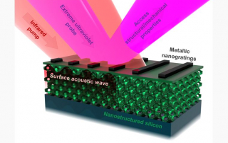
Extremely thin films of dielectrics and other materials play vital roles in many types of advanced microelectronics, but their tiny dimensions and atomic make-up can impair mechanical performance.

Now, researchers at the NSF STROBE Science and Technology Center in the U.S. have shown they can characterize the mechanical properties of silicon-carbide films as thin as 5 nm using tabletop sources of extreme ultraviolet laser light—showing them to be far softer than thicker films of the same material (Phys. Rev. Mater., doi: 10.1103/PhysRevMaterials.4.073603).

Scientists Open New Window into the Nanoworld

CU Boulder researchers have used ultra-fast extreme ultraviolet lasers to measure the properties of materials more than 100 times thinner than a human red blood cell. The team, led by scientists at JILA, reported its new feat of wafer-thinness this week in the journal Physical Review Materials. The group’s target, a film just 5 nanometers thick, is the thinnest material that researchers have ever been able to fully probe, said study coauthor Joshua Knobloch. “This is a record-setting study to see how small we could go and how accurate we could be,” said Knobloch, a graduate student at JILA, a partnership between CU Boulder and the National Institute of Standards and Technology (NIST). He added that when things get small, the normal rules of engineering don’t always apply. The group discovered, for example, that some materials seem to get a lot softer the thinner they become.

Reading the Secrets of the Nanoworld with Infrared Light

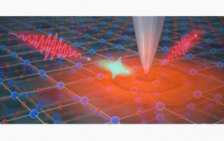
Many of the life’s elementary processes and material properties are determined by how molecules couple and interact. Until recently, it’s been impossible to see how these molecules interact with each other with a high enough resolution. The Raschke Group has used infrared lasers and a new microscope to get a high-resolution view of molecular coupling in porphyrin nanocrystals.

Congrats to James Utterback for Receiving the 2020 Arnold O. Beckman Postdoctoral Fellowship from the Beckman Foundation

The Arnold and Mabel Beckman Foundation announced today its 2020 class of Arnold O. Beckman Postdoctoral Fellows in Chemical Sciences, individuals who underscore the Foundation’s mission of supporting basic research in the chemical sciences and chemical instrumentation. They were selected after a three-part review led by a panel of scientific experts. The Foundation will award more than $4 million in funding over the next three years for 14 exceptional research fellows from 7 universities.

Full characterization of ultrathin 5nm low-k dielectric films: Influence of thickness and dopants on the mechanical properties

The demand for faster, more efficient, and more compact nanoelectronic devices, like smartphone chips, requires engineers to develop increasingly complex designs. To achieve this, engineers use layer upon layer of very thin films – as thin as only a couple strands of DNA – with impurities added, to tailor the function. However, the presence of these necessary impurities and extreme thinness degrades the material strength, reducing its performance and making it more likely to fail. To date, it was simply not possible to test the stiffness or compressibility of the thinnest of these ultra-thin films. Now, by using laser-like beams at very short wavelengths – beyond the ultraviolet region of the spectrum – scientists were finally able to measure the mechanical properties of these films. What they learned was surprising: as the layers thinned, the mechanical properties dramatically deteriorated, becoming nearly 10 times flimsier than expected. Additionally, the presence of impurities can be more detrimental to the film’s strength than the effect of its thinning. These findings will influence the design of next generation electronic and other nanoscale devices.

Congrats to Leo Hamerlynck for Receiving a National Defense Science and Engineering Graduate Fellowship

The National Defense Science and Engineering Graduate (NDSEG) Fellowship is a highly competitive, portable fellowship that is awarded to U.S. citizens and nationals who intend to pursue a doctoral degree in one of fifteen supported disciplines. NDSEG confers high honors upon its recipients, and allows them to attend whichever U.S. institution they choose. NDSEG Fellowships last for three years and pay for full tuition and all mandatory fees, a monthly stipend, and up to $1,000 a year in medical insurance (this excludes dental and vision insurance).

The Department of Defense (DoD) is committed to increasing the number and quality of our nation’s scientists and engineers, and towards this end, has awarded nearly 3,400 NDSEG fellowships since the program’s inception in 1989. The NDSEG Fellowship is sponsored by the Air Force Office of Scientific Research (AFOSR), the Army Research Office (ARO), and the Office of Naval Research (ONR), under the direction of the Director of Defense Research and Engineering (DDR&E).

Researchers Capture Crystal Nucleation with Atomic Resolution in 4D (3D Plus Time)

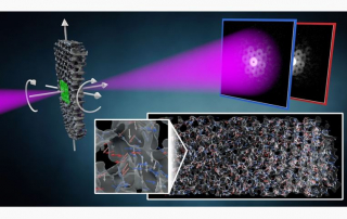
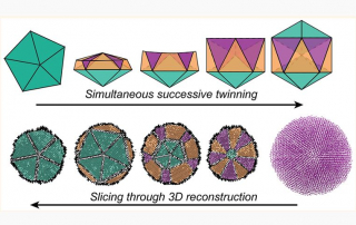
A team of scientists has developed four-dimensional (the three dimensions of space plus the fourth dimension of time) atomic electron tomography. Tomography is a technique for creating images of cross sections of an object using X-rays or ultrasound. The technique directly images the dynamics of structural changes at the atomic scale during nucleation. Nucleation is the creation of structure in a vapor, solution, or liquid. The scientists found that the nuclei came in a broad range of shapes and sizes and possess a diffuse interface surrounding a stable core. Their observations challenge the long-held classical nucleation theory that posits nucleation begins with the formation of perfectly spherical nuclei that grow after they reach a certain critical size.

Understanding the Role of Molecular Disorder in Organic Electronics and Photonics

How molecules interact and transfer energy between each other dictates the performance in molecular electronics, organic light emitting diodes, photovoltaics, or in many biological processes. However, imaging the controlling underlying molecular order and associated wavefunction delocalization on the molecular scale has long remained a major challenge in imaging science.

A STROBE team from CU Boulder, UC Berkeley and LBNL, has overcome this challenge developing a new technique of nanoimaging in the infrared probing the delicate low-energy landscape of molecular interactions. Measuring coupled molecular vibrations with high precision provides for a new molecular ruler to resolve the effect of disorder with sub-nanometer resolution. In a representative organic electronic material of metal-porphyrin nano-crystals the researchers learned about the relationship between structure and function of energy transfer on molecular length scales. The new insights gained advance our understanding of light harvesting in photosynthesis and improve the design of next generation organic electronic and photonic devices.

Imaging Material Functionality Through Three-dimensional Nanoscale Tracking of Energy Flow

The next generation of semiconducting materials that will facilitate energy transport and storage in the technologies around us is becoming increasingly complex. The ability of energy carriers to move between atoms and molecules underlies biochemical and material function. Understanding and controlling energy flow, however, requires observing it on ultrasmall and ultrafast spatio-temporal scales, where energetic and structural roadblocks dictate the fate of energy carriers.

A STROBE team led by Naomi Ginsberg (UCB) developed a novel time-resolved interferometric scattering microscope to visualize how energy navigates the intrinsically disordered landscapes in these materials on the nanoscale. With this high-throughput technique, they collected non-invasive stroboscopic movies in a variety of organic, inorganic, and hybrid materials to demonstrate its powerful versatility. Applied to other cutting-edge materials, we hope to inform the design of new functional devices for the semiconductor industry of tomorrow.

Go to Top