masonlw

Home \ Lauren Mason

About Lauren Mason

This author has not yet filled in any details.
So far Lauren Mason has created 285 blog entries.

Congratulations to Giulia Mancini for Receiving the International Union of Pure and Applied Physics (IUPAP) Young Scientist Prize in Optics from the International Commission of Optics

Congratulations to Giulia Mancini for receiving the IUPAP Young Scientist Prize in Optics! In 2005 the International Union of Pure and Applied Physics (IUPAP) created the Young Scientist Prizes for its commissions. The international Commission of Optics (ICO), as an Affiliated Commission of IUPAP, decided in 2008 to adopt the IUPAP Young Scientist Prize in Optics. The IUPAP prize in optics will be awarded annually through ICO to a scientist who has made noteworthy contributions to applied optics and photonics during a maximum of 8 years of research experience after having earned a PhD degree. Career interruptions will not be counted as time of research experience.

Infrared nano-imaging and -spectroscopy: methods, applications, and current research

Infrared (IR) vibrational scattering scanning near-field optical microscopy (s-SNOM) has advanced to become a powerful nano-imaging and -spectroscopy technique to probe molecular and lattice vibrations, low-energy electronic excitations and correlations, and related collective surface plasmon, phonon, or other polaritonic resonances. s-SNOM enables the study of complex heterogeneous materials with simultaneous nanoscale spatial resolution and quantum state spectroscopic specificity. It has also been extended to studying dynamics in the time domain, where ultrafast vibrational and electronic spectroscopy unravels mechanisms underlying functionality in quantum materials. I will discuss light sources, implementations of nano-probe spectroscopy and imaging, and open scientific questions that are being addressed with these techniques.

Pycro-Manager: open-source software for customized and reproducible microscope control

Innovative microscopy techniques are often impeded by a lack of control software that is capable of meeting demands for speed and performance, integrating new and diverse types of hardware, providing the flexibility to adapt in real time to the data being captured, and providing user-friendly programming interfaces. As a result, researchers often end up developing custom software that works only with specific instruments, using closed-source and/or proprietary programming languages. Pycro-Manager is a package that meets these challenges by enabling python control of Micro-Manager (an open-source microscopy control software) as well as the simple development of customized experiments that involve microscope hardware control integrated with real-time image processing. It is compatible with hundreds of microscope components and full microscopes and provides open source APIs for the integration of new hardware. More information can be found at: https://pycro-manager.readthedocs.io/en/latest/

Tutorial: X-ray microscopy and spectroscopy at synchrotron light sources

Synchrotron light sources provide unique types of X-rays and different end-station configurations. As such, synchrotrons can host a wide variety of experiments to study the most diverse materials and their properties. In this talk, we will discuss the benefits and challenges of these light sources in the context of x-ray microscopy. We will provide examples of what they can be used for, including spectromicroscopy for 3D magnetic imaging and elemental analysis, while focusing on the COherent Scattering and MICroscopy (COSMIC) beamline located at the Advanced Light Source, Lawrence Berkeley National Laboratory (LBNL).

2D vibrational exciton nano-imaging of domain formation in self-assembled monolayer

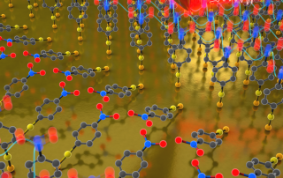
Understanding the chemical and physical properties of surfaces at the molecular level is highly relevant in the fields of medicine, semiconductors, batteries, etc. where precise atomic level control of determines materials and device performance. In particular, molecular order and domains affect many of the desired functional properties with carrier transport, wettability, and chemical reactivity often controlled by intermolecular coupling. However, both imaging of molecular surfaces and spectroscopy of molecular coupling has long been challenged by limited chemically specific contrast, spatial resolution, sensitivity, and precision. In this work, a team of  STROBE researchers demonstrate vibrational excitons as a molecular ruler of intermolecular coupling and quantum sensor for wave function delocalization to image nanodomain formation in self-assembled monolayers. In novel precision spatio-spectral infrared scattering scanning near-field optical microscopy combined with theoretical modelling few nanometer domain sizes and their distribution across micron scale fields of view could be resolved. This approach of vibrational exciton nanoimaging is generally applicable to study structural phases and domains in a wide range of molecular interfaces and the method can be used for engineering better molecular interfaces, with controlled properties for molecular electronic, photonic, or biomedical applications.

STROBE Seminar: Patent Law and Intellectual Property

This seminar will include a brief discussion of patents and patent law including the purposes of patents (such as licensing, assets of a company, something to put on your resume), how they are structured (and how they are different from scientific papers), and careers in the patent law field.

About the speaker: Jennifer Bales has a BS in engineering from California State University Northridge and an MS in electrical engineering, specializing in optics, from University of Southern California.  Before going to law school at the University of Colorado, she worked in aerospace in the fields of ECCM, infrared image processing, and synthetic aperture radar (SAR) ground stations.  Her current patent work emphasizes optics, image processing, and signal processing, along with thermodynamics (in the area of refrigeration and air conditioning), medical devices, and various other electrical and mechanical inventions. She has been working as a patent attorney for over twenty years and has helped clients attain over 100 patents.

Cool it: Nano-scale discovery could help prevent overheating in electronics

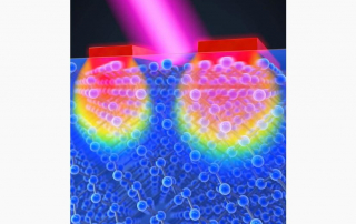
A team of physicists and engineers at CU Boulder have solved the mystery behind a perplexing phenomenon in the nano realm: why some ultra-small heat sources cool down faster if you pack them closer together. The research began with an unexplained observation: a team led by Margaret Murnane and Henry Kapteyn at JILA were experimenting with metallic nanolines on a silicon substrate that when heated with a laser, something strange occurred. Nanoscale heat sources do not usually dissipate heat efficiently. But if you pack them close together, they cool down much more quickly.

Now, the researchers know why it happens. The team joined forces with a group of theorists led by Mahmoud Hussein in Aerospace Engineering Sciences to use computer-based simulations to track the passage of heat from their nano-sized bars. The simulations were so detailed that they could follow the behavior of each and every atom in the model—millions of them in all. They discovered that when they placed the heat sources close together, the vibrations of energy (called phonons) they produced bounced off each other more efficiently when other heat sources were nearby, scattering heat away and cooling the bars down.

The group’s results highlight a major challenge in designing the next generation of tiny devices, such as microprocessors or quantum computer chips. When you shrink down to very small scales, heat does not always behave the way you think it should.

Seeing with the “Nano” Eye

Understanding the chemical and physical properties of surfaces at the molecular level has become increasingly relevant in the fields of medicine, semiconductors, rechargeable batteries, etc. For example, when developing new medications, determining the chemical properties of a pill’s coating can help to better control how the pill is digested or dissolved. In semiconductors, precise atomic level control of interfaces determines performance of computer chips. And in batteries, capacity and lifetime is often limited by electrode surface degradation.  These are just three examples of the many applications in which the understanding of surface coatings and molecular interactions are important.

The imaging of molecular surfaces has long been a complicated process within the field of physics. The images are often fuzzy, with limited spatial resolution, and researchers may not be able to distinguish different types of molecules, let alone how the molecules interact with each other. But it is precisely this–molecular interactions–which control the function and performance of molecular materials and surfaces.  In a new paper published in Nano Letters, JILA Fellow Markus Raschke and graduate student Thomas Gray describe how they developed a way to image and visualize how surface molecules couple and interact with quantum precision. The team believes that their nanospectroscopy method could be used for molecular engineering to develop better molecular surfaces, with controlled properties for molecular electronic, photonic, or biomedical applications.

Congratulations to Mary Scott for Being named the Ted Van Duzer Endowed Professor in the UC Berkeley Department of Materials Science & Engineering

Congratulations to Mary Scott for Being named the Ted Van Duzer Endowed Professor in the UC Berkeley Department of Materials Science & Engineering. This professorship supports the work of a “promising non-tenured Professor in the College of Engineering”. The award also comes with financial support for Professor Scott’s research and students. The professor is named for Professor Ted Van Duzer, who is currently a Professor Emeritus in the Department of Electrical Engineering and Computer Sciences at Berkeley. Congratulations to Professor Scott for this wonderful and highly-deserved honor.

Tutorial: Electron Microscopy: Introduction, Applications and Opportunities

Electron microscopy is a high-resolution suite of characterization techniques used in the physical and biological sciences. By accelerating electrons to relativistic speeds (i.e. 0.5c) such that their characteristic wavelengths are 100,000 times smaller than visible light, one can perform high-resolution imaging down to the atomic scale. Furthermore, by implementing an array of diffraction and spectroscopic methods, electron microscopy can be used to decipher the nanoscale structure and composition of materials. This tutorial will begin by introducing electron microscopy and highlighting its advantages and disadvantages over visible and x-ray characterization techniques. Following this, the applications of electron microscopy will be summarized, with a specific focus on the cutting-edge experiments being performed by members of the STROBE community.

Go to Top