masonlw

Home \ Lauren Mason

About Lauren Mason

This author has not yet filled in any details.
So far Lauren Mason has created 240 blog entries.

Congrats to Charles Dove for Receiving a Hertz Fellowship

Charles Dove uses artificial intelligence (AI) to harness the physics of light. A PhD student in electrical engineering at the University of California, Berkeley, Charles uses principles from machine learning and differentiable programming to create new methods for the simulation and fully automatic design of light-based technology. This capability would enable significant growth in the scale, scope, and capabilities of nearly all light-based technology, including biomedical imaging, cellular manipulation and characterization, optical telecommunications, photonic quantum computing, and LIDAR.

A researcher in AI since his freshman year at Clemson University, Charles is the inventor of multiple technologies that combine electromagnetic wave physics and machine learning. His method for the efficient recovery of blood-flow information from scattered laser light is currently being evaluated for potential use in optometry and brain surgery, and his method for 3D artificial vision through multi-frequency scattering offers a promising and practical alternative to conventional LIDAR.

Atomic structures determined from digitally defined nanocrystalline regions

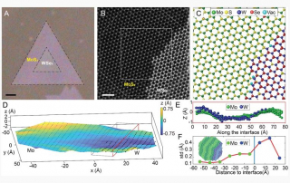
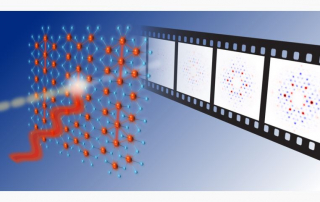
Three-dimensional (3D) structures of molecules determined from nanoscale regions of crystalline arrays could potentially illuminate the subtle differences that engender crystal defects or the multiple states accessible to subpopulations of molecules within an ensemble. A step toward this goal involves the extraction of meaningful diffraction data from 3D regions on the nanoscale. This is achieved using a near-parallel electron beam designed to illuminate sub-10nm regions of a sample. Scanning such a beam across a sample allows for digital logic to be applied to the measured data, facilitating the expostfacto assortment of information and reduction from desired 3D subvolumes.

A STROBE team from UCLA, UC Berkeley and LBNL collaborated to determine the first molecular structures determined by 4DSTEM. The structures were determined from a digitally defined subregion of a nanocrystal. After collecting TB of data, the team obtained reconstructions that revealed the atomic structure of a peptide, and showed that radiation damage imparted on the sample during data collection was not prohibitive for structure determination. Compared to other approaches, the approach allows for a much greater degree of control and obviates the need for spatial separation of samples. New methods, algorithms, enhanced microscopes and advanced sample preparation techniques developed by the STROBE collaboration were key to enabling the success of this project.

Compressive and adaptive nano imaging for enhanced speed and content

Scattering scanning near-field optical microscopy (s-SNOM) provides for spectroscopic imaging from molecular to quantum materials with few nanometer deep sub-diffraction limited spatial resolution. However, conventional acquisition methods are often too slow to fully capture a large field of view spatio-spectral dataset. Through this collaboration, STROBE researchers, at CU Boulder and the ALS –Berkeley, demonstrated how the data acquisition time and sampling rate can be significantly reduced while maintaining or even enhancing the physical or chemical image information content. The novel data acquisition and mathematical concepts implemented are based on advanced data compressed sampling, matrix completion, and adaptive random sampling. This research is of particular interest in synchrotron based nano-imaging facilities. This work paves the way to true spatio-spectral chemical and materials nano-spectroscopy with a reduction of sampling rate by up to 30 times.

New phase retrieval methods enabled by the world’s fastest electron detector

The need for rapid and accurate image analysis is increasing in electron microscopy studies of nanomaterials. With newly developed fast, high-efficiency electron detectors and automated imaging protocols, incorporating electron microscopy into high throughput materials design efforts is becoming possible. These new capabilities strongly motivate automated methods to extract relevant structural features, such as nanoparticle size, shape, and defect content, from high resolution transmission electron microscopy (HRTEM) data to link these features to bulk properties and study the influence of heterogeneity on bulk behavior. In general, protocols that surpass the accuracy of traditional image analysis and do not require time-consuming manual analysis are needed. Recent advances in image interpretation using deep learning using machine learning make it a promising route toward automatic interpretation of HRTEM micrographs.

In this STROBE collaboration, we demonstrate a pipeline to detect and classify regions of interest in HRTEM micrographs. Our pipeline uses a convolutional neural net (CNN) to identify crystalline regions (nanoparticles) from an amorphous background in the images, and then feeds individual regions of interest into a random forest classifier to detect whether or not they contain a crystallographic defect. Our CNN has a lightweight U-Net architecture and accurately segments a diverse population of nanoparticles with only a small number of training images. After segmentation, individual nanoparticle regions can be isolated and fed directly into existing python tools to extract size and shape statistics. To detect the presence of defects in nanoparticle regions, we implement a random forest classifier. We demonstrated the random forest classifier’s ability to detect stacking faults in the CdSe subset of identified nanoparticles. Both the CNN and classifier demonstrate state of the art performance at their respective tasks. While this work focuses on HRTEM images of nanoparticles supported on a carbon substrate, in principle the tool can be used to detect any regions of crystallinity in HRTEM data.

Nondestructive, high-resolution, chemically specific 3D nanostructure characterization using phase-sensitive EUV imaging reflectometry

Next-generation nano and quantum devices have increasingly complex 3D structure. As the dimensions of these devices shrink to the nanoscale, their performance is often governed by interface quality or precise chemical or dopant composition. A STROBE team from CU Boulder, UCLA, UC Berkeley, as well as laser and nanoelectronics industry partners, worked together for 4 years to design, construct and commission the first phase-sensitive extreme ultraviolet imaging reflectometer. It combines the excellent phase stability of tabletop coherent extreme UV (EUV) light sources, the unique chemical- and phase-sensitivity of coherent EUV imaging, and state-of-the-art algorithms. This tabletop microscope can non-destructively probe surface topography, layer thicknesses, and interface quality, as well as dopant concentrations and profiles. High-fidelity imaging was achieved by implementing phase sensitive imaging at different angles, by using advanced methods to mitigate noise and artifacts in the reconstructed image, and by using a high-brightness, EUV source with excellent intensity and wavefront stability. These measurements were validated through multiscale electron and atomic force microscopy imaging to show that this approach has unique advantages compared with others. Critical to this project were new photon and electron-based imaging methods, advanced algorithms, unique samples, as well STROBE advances in tabletop coherent imaging in transmission and reflection mode. Several STROBE trainees received awards for this effort.

Investigating the potential for entangled two-photon excited fluorescence imaging

Setting bounds on the absorption cross-sections of molecular systems. There has been a long-running controversy regarding the “quantum advantage” for multiphoton excitation of molecules with entangled photons and if quantum multiphoton imaging can be realized. Although theoretical proposals have been advanced for decades, no experimental work (with the exception of a publication by Jeff Kimble’s group in the 1990s) appeared in the literature until 2006 when reports from a small number of groups began to emerge of a large quantum enhancement (e.g. up to 10 orders of magnitude) of the two photon excitation rate using entangled pairs compared to classical light. Last year, a paper describing a microscope based on the “entangled two-photon absorption” (E2PA) effect was published in Journal of the American Chemical Society. On the other hand, it has emerged from discussions at scientific meetings that many researchers have failed to replicate the results in these numerous publications, or to find any other evidence for this enhancement. As a result, there is considerable skepticism of the publications making these remarkable claims. Unfortunately, these negative results haven’t been published and therefore a rigorous basis for resolving the controversy hasn’t yet been established. Finally, new experiments at JILA have finally set upper-bounds for the E2PA cross-sections in molecular fluorophores, including those investigated in previous reports. We performed both classical and quantum light excitation in the same optical transmission and fluorescence-based systems with rigorously characterized states of light and measurement sensitivities. We find that E2PA cross-sections are at least four to five orders of magnitude smaller than previously reported. Our results imply that the signals and images reported in previous publications are artifacts. Although we don’t expect this contribution to be the last word on the subject, this work introduces a new level of experimental rigor that will lead towards new designs for quantum microscopes and sensors.

Go to Top