masonlw

Home \ Lauren Mason

About Lauren Mason

This author has not yet filled in any details.
So far Lauren Mason has created 240 blog entries.

Industrial Applications of Ultrafast Lasers I: Basic Physics and Examples

Critical to the design and development of present and future semiconductor and quantum devices is the full understanding of the electronic structure of the materials that comprise the complex functional stacks in a non-destructive way. In Seminars I and II, I will describe the application of femtosecond ultraviolet photoelectron and photovoltage spectroscopy (fs UPPS) to fully characterize the electronic structure of industrially important materials and devices. The addition of fs photovoltage spectroscopy, which extracts the underlying semiconductor substrate band bending provides virtually complete characterization of the electronic structure of complex device material stacks. This includes Fermi level location, valence band locations and offsets, oxide properties and charging as a function of processing, and tunnel barrier heights to name a few. In the first seminar I will describe the methodology and physics of this spectroscopic approach. In the Seminar II, I will describe specific material and device studies of key industrial interest; these include high-K/metal gate MOS devices, earth abundant thin film photovoltaics, the Al2O3 tunnel barrier utilized in quantum computing transmons, organic LEDs and phase change materials for neuromorphic/AI applications. Additional seminars, if interested would include further examples (earlier studies of electron dynamics at surfaces and interfaces) and femtosecond ablative photomask repair.

3D atomic details of next-generation alloys revealed for first time

Alloys, which are materials such as steel that are made by combining two or more metallic elements, are among the underpinnings of contemporary life. They are essential for buildings, transportation, appliances and tools — including, very likely, the device you are using to read this story. In applying alloys, engineers have faced an age-old trade-off common in most materials: Alloys that are hard tend to be brittle and break under strain, while those that are flexible under strain tend to dent easily.

Possibilities for sidestepping that trade-off arose about 20 years ago, when researchers first developed medium- and high-entropy alloys, stable materials that combine hardness and flexibility in a way in which conventional alloys do not. (The “entropy” in the name indicates how disorderly the mixture of the elements in the alloys is.)

Congrats to Nicholas Jenkins for Being Named as the 2024 Recipient of the SPIE Nick Cobb Memorial Scholarship

Nicholas Jenkinshas been announced as the 2024 recipient of the $10,000 Nick Cobb Memorial Scholarship by SPIE, the international society for optics and photonics, and Siemens EDA — formally Mentor, a Siemens company — for potential contributions to advanced lithography or a related field. Jenkins will also be honored during 2024’s SPIE Advanced Lithography + Patterning conference.

The Nick Cobb scholarship recognizes an exemplary graduate student working in the field of lithography for semiconductor manufacturing. The award honors the memory of Nick Cobb, who was an SPIE Senior Member and chief engineer at Mentor. His groundbreaking contributions enabled optical and process proximity correction for IC manufacturing. Originally funded for three years ending in 2021, the Nick Cobb Scholarship will be awarded to one student annually for an additional period of three years, through 2024.

Jenkins is pursuing a PhD in Physics at JILA and the University of Colorado, Boulder (CU). His research, under the guidance of Margaret Murnane and Henry Kapteyn, focuses on the precise fabrication and metrology of nanomaterials and devices to advance science and technology in areas such as nanoelectronics and metamaterials. As a final-year PhD student, Jenkins leads several experimental campaigns to use extreme ultraviolet (EUV) scatterometry and imaging in order to more precisely measure the structure and composition of nanoscale objects. Jenkins received his BS in Physics, summa cum laude, from the University of Colorado, Colorado Springs, in 2018, and his MS in Physics from the University of Colorado, Boulder, in 2021. He won the 2022 Colorado Photonics Industry Student Poster Contest, is currently working on projects for Samsung, 3M, and the Moore Foundation, and excels in his commitment to mentoring others.

“I’m honored to receive the Nick Cobb Memorial Scholarship and I’m excited for the opportunity to share my research with others in the field at the upcoming SPIE Advanced Lithography + Patterning meeting,” notes Jenkins. “The metrology community has continued to help push forward what humans are capable of on the nanoscale, and I’m glad to be part of the effort.”

Encoding information using optical imaging systems in the AI era

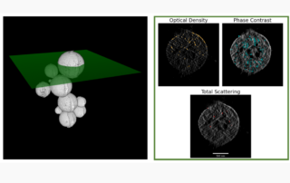
Abstract: The advent of artificial intelligence, particularly deep neural networks, is transforming the traditional criteria used to evaluate imaging systems. Increasingly, algorithms are used to process captured data, yielding outputs with little perceptual resemblance to its original form. This change broadens the scope of design possibilities while also creating a new challenge to define what constitutes a “good” imaging device when human interpretability is no longer a requirement. In this talk, we address this challenge using a probabilistic modeling approach, which can be used to quantify the information content of images captured under various conditions. We apply this framework to various imaging modalities, including label-free LED-array microscopy, lensless cameras, and single-shot 3D fluorescence microscopy, showing how it can directly evaluate performance without the need for labor-intensive post-processing algorithm development. This framework provides a new set of design principles uniquely tailored for the AI era.

Speaker Bio: I am a part-time postdoctoral researcher at UC Berkeley in the Computational Imaging Lab with Prof. Laura Waller in the Department of Electrical Engineering and Computer Sciences, where I received my PhD in Computational Biology and MS in Electrical Engineering and Computer Sciences. I am also the founder of Photomics, Inc., where I create open-source software for microscope control and label-free, computational microscopes. My research is focused on the design of hardware, software, and algorithms for data and information-driven design and control of optical microscopes. This work draws from many fields, including optical physics, machine learning, single-cell biology, immunology, software engineering, data science, computer vision, and information theory. More details can be found in the research section.

Imaging with multimode fiber endoscopes

Abstract:  In-vivo imaging through multimode fibers has been recently accomplished. Multimode fibers are attractive for endoscopic applications due to their thin cross-section, a large number of degrees of freedom, and flexibility. However modal dispersion and intermodal coupling preclude direct image transmission. The development of fast spatial phase control enables focus scanning and structured illumination for different novel imaging modalities. We discuss the implications of these techniques for ultrathin optical endoscopy.

Speaker Bio: Prof. Rafael Piestun received the Ingeniero Electricista degree from the Universidad de la República (Uruguay) and MSc. and Ph.D. degrees in Electrical Engineering from the Technion – Israel. From 1998 to 2000 he was a researcher at Stanford University. Since 2001 he has been at the University of Colorado Boulder where is a professor in the department of Electrical and Computer Engineering and in the Physics department. He is a fellow of the Optical Society of America, was a Fulbright scholar, an Eshkol fellow, received a Honda Initiation Grant award, a Minerva award, a Provost Achievement Award, and El-Op and Gutwirth prizes. He was associate editor of Optics and Photonics News and Applied Optics. He is founder of the company Double Helix Optics (SPIE Prism Award, First Place in the Luminate Competition) and the company Modendo Inc. His areas of interest include computational optical imaging, superresolution microscopy, volumetric photonic devices, scattering optics, and ultrafast optics.

‘Doughnut’ beams help physicists see incredibly small objects

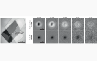
In a new study, researchers at CU Boulder have used doughnut-shaped beams of light to take detailed images of objects too tiny to view with traditional microscopes.

The new technique could help scientists improve the inner workings of a range of “nanoelectronics,” including the miniature semiconductors in computer chips. The discovery was highlighted Dec. 1 in a special issue of Optics & Photonics News called Optics in 2023.

The research is the latest advance in the field of ptychography, a difficult to pronounce (the “p” is silent) but powerful technique for viewing very small things. Unlike traditional microscopes, ptychography tools don’t directly view small objects. Instead, they shine lasers at a target, then measure how the light scatters away—a bit like the microscopic equivalent of making shadow puppets on a wall.

So far, the approach has worked remarkably well, with one major exception, said study senior author and Distinguished Professor of physics Margaret Murnane.

“Until recently, it has completely failed for highly periodic samples, or objects with a regularly repeating pattern,” said Murnane, fellow at JILA, a joint research institute of CU Boulder and the National Institute of Standards and Technology (NIST). “It’s a problem because that includes a lot of nanoelectronics.”

4D Scanning Transmission Electron Microscopy for Multimodal and Multiscale Materials Characterization

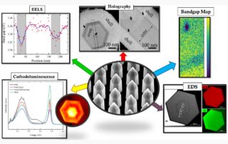
Abstract: Physical properties of matter depend on structure across vastly disparate length scales, from well below the atomic to macroscopic.  In this talk, we’ll discuss scale-bridging scanning transmission electron microscopy (STEM) experiments and the algorithms used to quantify them, measuring quantities from picometer deformations of individual atomic columns in charge density wave materials under in-situ cryogenic cooling, to grain orientations of hundreds of crystallites in a single capture, to lattice parameter variations measured across the many micron lengths of LixFePO4 nanoplatelets in several stages of electrochemical cycling. Many of these datasets are large, and integrating computation and experiment is necessary in each case.  In atom tracking with high-angle annular dark-field (HAADF)-STEM, instabilities and bubbling from the cryogen can easily spoil in-situ measurements – by combining many fast-acquisition low-signal image captures with a registration algorithm tailored to nearly uniform lattices, measuring and visualizing ~pm lattice displacements in low-temperature CDW phases is possible.  In 4D-STEM, in which a 2D image of the diffracted electrons is collected at each position of the 2D beam raster, matching algorithms to experiment remains essential to make sense of the large and information rich datasets.  Examples will be selected to highlight a range of modalities, methodologies, and applications, and will include Bragg localization, amorphous/crystal classification, phase identification, automated crystal orientation mapping, and others.

Speaker Bio: Ben Savitzky is a postdoctoral scientist at the National Center for Electron Microscopy in Berkeley CA.  He created, maintains, and leads development of py4DSTEM, a Python software package for 4D-STEM data analysis.  He completed his PhD with Lena Kourkoutis and Cornell University in 2018.

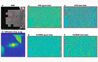
High-Fidelity Ptychography of Highly Periodic Structures

Lensless imaging based on ptychographic coherent diffractive imaging enables diffraction-limited microscopy at short wavelengths, overcoming the limits of imperfect optics.1,2 Ptychographic imaging of highly periodic structures has been challenging, however, due to the lack of diversity in the recorded diffraction patterns, which leads to poor convergence of the reconstructed sample images. Although techniques (such as modulus enforced probe and total variation regularization) have been explored to address this challenge, they suffer from slow convergence, heavy reliance on constraints on the samples, or both. This significantly limits ptychography’s application to a wide variety of periodic structures in photonics, nanoelectronics and extreme ultraviolet (EUV) photomasks.

Ab initio structures from nanocrystal molecular lattices

Electron diffraction has dramatically increased in popularity amongst chemists given its renewed application for ab initio structure determination from molecular nanocrystals. In one implementation, popularly referred to as 3D ED or MicroED, crystals nanocrystals orders of magnitude too small for conventional X-ray analysis are interrogated by an electron beam to determine atomic structures. However, these approaches are thwarted by disordered, overlapping, or otherwise poorly diffracting domains.

Spatially resolved diffraction mapping techniques can overcome some of these limitations, and have seen limited application in X-ray diffraction. In electron microscopy, such approaches, including 4D scanning electron microscopy (4D-STEM), have grown popular. We demonstrated that 4D-STEM can be used to determine ab initio structures of molecules by direct methods, from small ordered nanodomains of single microcrystals. In our approach 4D-STEM is used to generate diffraction scans that enable ex post facto reconstruction of digitally defined virtual apertures. The synthetic patterns derived from these scans are suitable for direct methods phasing of molecular structures.

In addition, this approach unveils that coherently diffracting zones (CDZs) in molecular crystals form unpredictably distributed striations. The observation of these zones and our ability to determine structures from these regions of nanocrystals empowers us to explore their atomic substructure and their response to radiolytic damage.

Go to Top