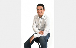
masonlw

Home \ Lauren Mason

About Lauren Mason

This author has not yet filled in any details.
So far Lauren Mason has created 288 blog entries.

Seeing with the “Nano” Eye

Understanding the chemical and physical properties of surfaces at the molecular level has become increasingly relevant in the fields of medicine, semiconductors, rechargeable batteries, etc. For example, when developing new medications, determining the chemical properties of a pill’s coating can help to better control how the pill is digested or dissolved. In semiconductors, precise atomic level control of interfaces determines performance of computer chips. And in batteries, capacity and lifetime is often limited by electrode surface degradation.  These are just three examples of the many applications in which the understanding of surface coatings and molecular interactions are important.

The imaging of molecular surfaces has long been a complicated process within the field of physics. The images are often fuzzy, with limited spatial resolution, and researchers may not be able to distinguish different types of molecules, let alone how the molecules interact with each other. But it is precisely this–molecular interactions–which control the function and performance of molecular materials and surfaces.  In a new paper published in Nano Letters, JILA Fellow Markus Raschke and graduate student Thomas Gray describe how they developed a way to image and visualize how surface molecules couple and interact with quantum precision. The team believes that their nanospectroscopy method could be used for molecular engineering to develop better molecular surfaces, with controlled properties for molecular electronic, photonic, or biomedical applications.

Congratulations to Mary Scott for Being named the Ted Van Duzer Endowed Professor in the UC Berkeley Department of Materials Science & Engineering

Congratulations to Mary Scott for Being named the Ted Van Duzer Endowed Professor in the UC Berkeley Department of Materials Science & Engineering. This professorship supports the work of a “promising non-tenured Professor in the College of Engineering”. The award also comes with financial support for Professor Scott’s research and students. The professor is named for Professor Ted Van Duzer, who is currently a Professor Emeritus in the Department of Electrical Engineering and Computer Sciences at Berkeley. Congratulations to Professor Scott for this wonderful and highly-deserved honor.

Tutorial: Electron Microscopy: Introduction, Applications and Opportunities

Electron microscopy is a high-resolution suite of characterization techniques used in the physical and biological sciences. By accelerating electrons to relativistic speeds (i.e. 0.5c) such that their characteristic wavelengths are 100,000 times smaller than visible light, one can perform high-resolution imaging down to the atomic scale. Furthermore, by implementing an array of diffraction and spectroscopic methods, electron microscopy can be used to decipher the nanoscale structure and composition of materials. This tutorial will begin by introducing electron microscopy and highlighting its advantages and disadvantages over visible and x-ray characterization techniques. Following this, the applications of electron microscopy will be summarized, with a specific focus on the cutting-edge experiments being performed by members of the STROBE community.

Congratulations to Naomi Ginsberg for being elected as a 2021 APS Fellow

Congratulations to Naomi Ginsberg for being named a the innovative development of spatiotemporally resolved imaging and spectroscopy methods, and for their use in elucidating energy transport in hierarchical and heterogeneous materials, as well as in the formation and transformation of said materials.

The APS Fellowship Program was created to recognize members who may have made advances in physics through original research and publication, or made significant innovative contributions in the application of physics to science and technology. They may also have made significant contributions to the teaching of physics or service and participation in the activities of the Society.

Fellowship is a distinct honor signifying recognition by one’s professional peers. Each year, no more than one half of one percent of the Society’s membership (excluding student members) is recognized by their peers for election to the status of Fellow of the American Physical Society.

Three-dimensional atomic packing in amorphous solids with liquid-like structure

Liquids and solids are two fundamental states of matter. Although the structure of crystalline solids has long been solved by crystallography, our understanding of the 3D atomic structure of liquids and amorphous materials remained speculative due to the lack of direct experimental determination. Now, a collaborative team from UCLA, Lawrence Berkeley National Lab and Brown University has advanced atomic electron tomography to determine for the first time the 3D atomic positions in monatomic amorphous materials, including a Ta thin film and two Pd nanoparticles. Despite different chemical composition and synthesis methods, they observed that pentagonal bipyramids are the most abundant atomic motifs in these amorphous materials. Contrary to traditional understanding, most pentagonal bipyramids do not assemble icosahedra, but are closely connected to form networks extending to medium-range scales. Molecular dynamics simulations further revealed that pentagonal bipyramid networks are prevalent in monatomic metallic liquids, which rapidly grow in size and form more icosahedra during the quench from the liquid to the glass state. These results expand our fundamental understanding of the atomic structure of amorphous solids and will encourage future studies on amorphous-crystalline phase and glass transitions in non-crystalline materials with three-dimensional atomic resolution.

3D imaging study reveals how atoms are packed in amorphous materials

Many substances around us, from table salt and sugar to most metals, are arranged into crystals. Because their molecules are laid out in an orderly, repetitive pattern, much is understood about their structure.

However, a far greater number of substances — including rubber, glass and most liquids — lack that fundamental order throughout, making it difficult to determine their molecular structure. To date, understanding of these amorphous substances has been based almost entirely on theoretical models and indirect experiments.

A UCLA-led research team is changing that. Using a method they developed to map atomic structure in three dimensions, the scientists have directly observed how atoms are packed in samples of amorphous materials. The findings, published today in Nature Materials, may force a rewrite of the conventional model and inform the design of future materials and devices using these substances.

STROBE Nano-imaging center receives five-year, $22 million renewal from NSF

The National Science Foundation has renewed for five years and more than $22 million the cutting-edge Science and Technology Center on Real-Time Functional Imaging (STROBE). STROBE is developing the Microscopes of Tomorrow, and is a partnership between six institutions –– University of Colorado Boulder, UCLA, UC Berkeley, Florida International University, Fort Lewis College, and UC Irvine.

STROBE is advancing functional electron and light-based microscopies by integrating advanced algorithms, big data analysis and adaptive imaging to address issues that have the potential to transform imaging science and technology.

“The Vision of STROBE is to transform nanoscale imaging science and technology by developing the microscopes of tomorrow,” according to Margaret Murnane and Jianwei “John” Miao, the Director and Deputy Director of STROBE. Miao is a professor of physics at UCLA, and member of UCLA’s California NanoSystems Institute. Murnane is a Distinguished Professor at CU Boulder, and a Fellow of JILA, a joint institute between CU Boulder and NIST.

Group photo of STROBE center members at a retreat in November 2019.

Group photo of STROBE center members at a retreat in November 2019.

STROBE is pushing electron, X-ray and nano-optical imaging to their limits by integrating state-of-the-art microscopes, with advanced algorithms and big data. Multiscale and multimodal imaging of the same samples are needed to tackle major scientific challenges in quantum, energy, disordered and biological materials. Major scientific challenges include a fundamental understanding of how to design materials at the nanoscale to enable more efficient and robust nano, energy and quantum devices. Other important grand challenges include techniques for imaging disordered materials, or understanding how atoms rearrange themselves in 3-D during the glass transition. “Addressing these major scientific challenges requires the development of new multiscale microscopes and methods, and combining them with common samples, fast detectors, big data, advanced algorithms and machine learning — which could not be accomplished without a center,” Miao said.

STROBE also integrates cutting-edge research with education through the multidisciplinary training of a diverse workforce – with the important goal of preparing a diverse group of trainees for long-term STEM careers through coordinated team projects with academe, national laboratories and industry, new multidisciplinary degree programs, multiple opportunities for professional development and through long-term programs based on best practices for broadening participation in STEM. STROBE’s new techniques, algorithms and instrumentation are in high demand, and STROBE is engaging in multiple routes for knowledge transfer with 77 partners in the academic, national laboratories and industry sectors. Over 92 graduated student and postdoctoral scientists have graduated from STROBE, as well as >125 undergraduate scholars.

Prof. Naomi Ginsberg is the STROBE lead at UC Berkeley, Prof. Jessica Ramella-Roman leads the team at Florida International University, Prof. Kay Phelps is the lead at Fort Lewis College, while Prof. Franklin Dollar is the lead at UC Irvine.

NSF science and technology centers conduct innovative, potentially transformative, complex research and education projects involving world-class research through partnerships among academic universities and industrial organizations in important areas of basic research. STROBE 77 partners span 43 academic, 22 industry and 7 national laboratories, including DOE, NIST, Moderna, 3M, SRC, Intel, AMD and Ball Aerospace.

See STROBE.colorado.edu

Go to Top