About Lauren Mason
This author has not yet filled in any details.So far Lauren Mason has created 323 blog entries.
Congrats to Ruiming Cao for Receiving the Hitachi High-Tech Best Presentation Award at the SPIE Photonics West Conference
Hitatchi sponsors two High-Tech Best Presentation Awards in High-Speed Biomedical Imaging and Spectroscopy at the SPIE Photonics West Conference. Congratulations to Ruiming Cao for receiving this award in 2023!
Two Postdoctoral Fellow Research Positions with Prof. Chen-Ting Liao at Indiana University Bloomington
Two postdoctoral fellow positions available in physics/engineering at Indiana University Bloomington
—————————————————————————————————-
(1) A postdoctoral fellow position in classical- and quantum-enhanced imaging
Job Description. A postdoctoral fellow position is now available at the Department of Physics (or jointly at Department of Intelligent Systems Engineering), Indiana University, Bloomington, Indiana, U.S.A. This project uses spatial, temporal, wavefront, and polarization-structured light beams to mimic quantum imaging properties for biological applications. The project aims to conduct proof-of-concept experiments of enhanced imaging performance using optical coherence tomography (OCT) as the bioimaging modality. The overarching goal is to show that the new approaches could overcome and outperform existing OCT disadvantages, either for those based on classical supercontinuum light sources or single-photon quantum light sources. This experimental research will involve designing, developing, constructing, and characterizing several types of structured light, generating beams with entangled degrees-of-freedoms (dubbed classical entanglement of light or mode-entanglement). Then, these visible and near-infrared beams will be used to test Mach–Zehnder interferometry-like OCT imaging setup. Some simulations will be accompanied to verify and guide the experiments. In this exciting role, you will work under the direction of Prof. Chen-Ting Liao (physics) and Prof. Hui Min Leung (engineering).
Links to additional information which may be of interest:
https://www.indiana.edu/
https://physics.indiana.edu
https://engineering.indiana.edu
https://graduate.indiana.edu/support/postdoc.html
https://www.visitbloomington.com/
Required qualifications:
• Ph.D. in physics, chemistry, optics/photonics, electrical engineering, or related fields.
• Ph.D. candidates in the ABD (all but dissertation) status will also be considered.
• Proven track record in scientific research and development.
• Hands-on experience with lasers and optical setups.
• Experience with data analysis using Matlab, Python, etc.
• Excellence in research and strong communication skills.
• High degree of independence together with the ability to work in a collaborative environment.
• Good working knowledge of written and spoken English.
Preferred qualifications:
• Experience with structured light, quantum optics, and OCT.
• Some experience with optics/photonics simulations using ZEMAX, Lumerical FDTD.
• Some experience with nanofabrication such as e-beam lithography.
• Some experience of using software (Matlab, Python, LabVIEW) to automate experimental controls.
• Some experience of using software such as SolidWorks for experimental setup designs.
The initial appointment for this position will be for 12 months. Additional 12-24 month extensions will be available based on performance, mutual agreement and funding. A competitive salary along with a benefits package will be offered. The starting date is flexible. Minority, women, and international candidates are strongly encouraged to apply. Interested candidates should send their (i) CV (including completed degrees, list of publications, research experience and expertise), (ii) a Cover Letter (briefly summarizing qualifications, motivations, and interests in this position), and (iii) contact information of at least two references to Prof. Chen-Ting Liao (chenting.liao [at] gmail.com).
Indiana University is an equal employment and affirmative action employer and a provider of ADA services. All qualified applicants will receive consideration for employment based on individual qualifications. Indiana University prohibits discrimination based on age, ethnicity, color, race, religion, sex, sexual orientation, gender identity or expression, genetic information, marital status, national origin, disability status or protected veteran status. Indiana University is committed to excellence through diversity. Indiana University has a strong commitment to principles of diversity and in that spirit seeks a broad spectrum of candidates including women, minorities, and persons with disabilities, and encourages applications from candidates with diverse cultural backgrounds.
—————————————————————————————————-
(2) A postdoctoral fellow position in quantum VUV and EUV light generation
Job Description. A postdoctoral fellow position is now available at the Department of Physics, Indiana University, Bloomington, Indiana, U.S.A. The project aims to explore potential pathways to generate quantum entangled and/or squeezed short-wavelength light sources (wavelength 1-100 nm), including vacuum- and extreme-ultraviolet (VUV and EUV) light. The overarching goal is to test the feasibility of several potential methods, based on quantum optics, nonlinear optics, and ultrafast optics, to experimentally explore how to generate VUV and EUV light carrying nonclassical properties. The properties include single-photon or Fock states, entangled states (in photon numbers, polarizations, wavelengths, and delay times), amplitude/phase squeezed states, and/or bright squeezed vacuum states of light. This experimental research will involve developing, creating, and characterizing various classical and quantum light sources, including the technologies used for near-infrared, visible, and ultraviolet, to VUV/EUV light. In this exciting role, you will work under the direction of Prof. Chen-Ting Liao and in collaboration with other researchers.
Links to additional information which may be of interest:
https://www.indiana.edu/
https://physics.indiana.edu
https://engineering.indiana.edu
https://graduate.indiana.edu/support/postdoc.html
https://www.visitbloomington.com/
Required qualifications:
• Ph.D. in physics, chemistry, optics/photonics, electrical engineering, or related fields.
• Ph.D. candidates in the ABD (all but dissertation) status will also be considered.
• Proven track record in scientific research and development.
• Hands-on experience with pulsed lasers, optical setups, and vacuum technologies.
• Experience with data analysis using Matlab, Python, etc.
• Excellence in research and strong communication skills.
• High degree of independence together with the ability to work in a collaborative environment.
• Good working knowledge of written and spoken English.
Preferred qualifications:
• Good working knowledge and understanding of quantum optics and ultrafast optics.
• Some experience of using software (Matlab, Python, LabVIEW) to automate experimental controls.
• Some experience of using software such as SolidWorks for experimental setup designs.
The initial appointment for this position will be for 12 months. Additional 12-24 month extensions will be available based on performance, mutual agreement and funding. A competitive salary along with a benefits package will be offered. The starting date is flexible. Minority, women, and international candidates are strongly encouraged to apply. Interested candidates should send their (i) CV (including completed degrees, list of publications, research experience and expertise), (ii) a Cover Letter (briefly summarizing qualifications, motivations, and interests in this position), and (iii) contact information of at least two references to Prof. Chen-Ting Liao (chenting.liao [at] gmail.com).
Indiana University is an equal employment and affirmative action employer and a provider of ADA services. All qualified applicants will receive consideration for employment based on individual qualifications. Indiana University prohibits discrimination based on age, ethnicity, color, race, religion, sex, sexual orientation, gender identity or expression, genetic information, marital status, national origin, disability status or protected veteran status. Indiana University is committed to excellence through diversity. Indiana University has a strong commitment to principles of diversity and in that spirit seeks a broad spectrum of candidates including women, minorities, and persons with disabilities, and encourages applications from candidates with diverse cultural backgrounds.
Senior Machine Learning Design Engineer
My team is under the ASML Brion Product Engineering Group (PEG) organization, which is responsible for feasibility study, product definition/design, flow integration, performance testing, and early customer engagement. My team is currently focusing on applying machine learning (ML) and data science (DS) techniques into semiconductor applications. Here are two example products we are working on now: Context based wafer level grouping (CBWG) and machine learning based image quality enhancement (ML-IQE). In CBWG, we use traditional machine learning models (e.g., trees) to group wafers based on context information (e.g., fab routing) and then do fine control based on groups. For ML-IQE we apply the state-of-the-art deep learning models to enhance the images from our scanning electron microscope (SEM) equipment. All these ML/DS products are very critical to ASML’s business and bring tremendous values to our customers. We are actively looking for candidates w/ solid background in ML and DS to work with us on solving those real-world challenging problems using latest ML/DS techniques.
The hiring manager emphasized that: “The candidates don’t have to be a ML/DS expert, solid background on simulation/modeling/optimization will work as well.”
Congrats to Jessica Ramella-Roman for Being Elected as a 2024 Optica Fellow
Jessica Ramella-Roman has been elected as a Fellow of Optica for her pioneering contributions to the study of polarized light transport in biological media through experimental and computational approaches.
The Board of Directors of Optica (formerly OSA), Advancing Optics and Photonics Worldwide, recently elected 129 members from 26 countries to the Society’s 2024 Fellow Class. Optica Fellows are selected based on several factors, including outstanding contributions to research, business, education, engineering and service to Optica and our community.
Fellows are Optica members who have served with distinction in the advancement of optics and photonics. The Fellow Members Committee, led by Chair Ofer Levi, University of Toronto, Canada, reviewed 216 nominations submitted by current Fellows. The Committee extends its thanks to all of this year’s nominators and references. As Fellows can account for no more than 10 percent of the total membership, the election process is highly competitive. Candidates are recommended by the Fellow Members Committee and approved by the Awards Council and Board of Directors.
The new Fellows will be honored at Optica conferences and events throughout 2024.
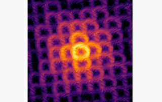
High-fidelity imaging of highly periodic structures enabled by vortex high harmonic beams
STROBE scientists solved a major imaging challenge by demonstrating high fidelity short wavelength imaging of highly-periodic structures for the first time, using engineered illumination via high harmonic extreme UV (EUV) beams carrying orbital angular momentum (OAM). This enables high-fidelity imaging and inspection of highly periodic structures for next-generation nano, energy and photonic devices.
Lensless imaging based on coherent diffractive imaging (CDI) enables near-perfect diffraction-limited microscopy at short wavelengths, overcoming the limits of imperfect and lossy optics. However, high fidelity imaging of highly periodic structures has been challenging. In CDI, a beam is scanned across a sample, and the scattered light is collected by a detector. A computer algorithm is then used to reconstruct an image of the sample. However, to retrieve high-fidelity images, the scatter patterns must change as the beam is scanned – which is not the case for highly periodic samples.
Graduate students Bin Wang and Nathan Brooks, working with Henry Kapteyn and Margaret Murnane, solved this long-standing challenge by using high harmonic beams carrying OAM. The high divergence and peak-intensity near their edges introduces strong interference fringes between adjacent diffraction orders in the far-field. These encode phase information into the scattered light as the beam is scanned, significantly enhancing diversity in the diffraction patterns so that the phase can be reliably retrieved. Moreover, defects in otherwise periodic grids can be more sensitively detected with improved signal-to-noise ratio > 100x, and with lower dose and sample damage than for scanning electron microscopy.
Visible laser beams carrying OAM (i.e. donut-shaped) beams revolutionized visible super-resolution microscopy. Now there is a path forward for bringing these powerful capabilities to shorter wavelengths.
Congrats to Ruiming Cao for Receiving best Student Paper Award at the Optica Imaging Congress
Ruiming Cao received the Best Student Paper Award for his paper titled, “Speckle Structured Illumination of Dynamic Samples with a Neural Space-time Model” at the Optica Imaging Congress this fall. Congratulations, Ruiming!
Congrats to Ke Xu for Being Selected as a Pew Innovation Fund Investigator
The Pew Scholars Program in the Biomedical Sciences provides funding to young investigators of outstanding promise in science relevant to the advancement of human health. The program makes grants to selected academic institutions to support the independent research of outstanding individuals who are in their first few years of their appointment at the assistant professor level. Congratulations to Ke Xu for being selected as a Pew Innovation Fund Investigator!
Congrats to Ke Xu for Receiving a Heising-Simons Faculty Fellowship
The Heising-Simons Faculty Fellows Program catalyzes scientific discovery by investing in high-risk, high-reward research directions. The Program supports exceptional faculty working on topics in a diverse set of fields, including astronomy, physics, geology and geophysics, materials sciences (in both physics and engineering), and physical and materials chemistry. Program awards will focus on creative and novel approaches that promise to lead to important scientific breakthroughs contributing to a greater understanding of the universe and its components, from the molecular and atomic to the geological and planetary scales, among other areas. Awards also fund the development of new tools, techniques and measurements that help probe these physical phenomena in new ways.
The Heising-Simons Faculty Fellows awards will be made to two UC Berkeley faculty members each year. Each $1M faculty award will be distributed over a period of five years. All early- and mid-career UC Berkeley faculty regardless of their home department are eligible to apply.
Prof. Xu’s project is “Single-Molecule Electrophoresis Microscopy”.
Congrats to Markus Raschke for Receiving a Research Collaboration Award from the University of Bayreuth Centre of International Excellence
Markus Raschke received an award from the University of Bayreuth Centre of International Excellence to foster collaborations. The project is titled “Pico-cavity QED.” The goal of this project between the Raschke group at the University of Colorado and the Lippitz group (Experimental Physics III) at the University of Bayreuth is to develop quantum-coherent systems operating at room temperature, taking advantage of recent developments in both groups of pico-cavity quantum electrodynamics (cQED) in tip-enhanced strong coupling and with plasmonic nanostructures. Congratulations, Markus!


