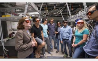
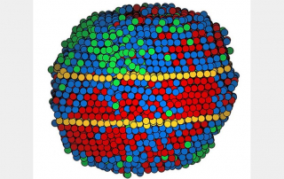
STROBE in the News

Home \ News \ STROBE in the News

Ripples in Space-Time: Nano-Imaging Functional Materials at their Elementary Scales

April 25, 2022|JILA, CU Boulder|

Functional materials—like molecular electronics, biomaterials, light-emitting diodes, or new photovoltaic materials—gain their electronic or photonic properties from complex and multifaceted interactions occurring at the elementary scales of their atomic or molecular constituents. In addition, the ability to control the functions of these materials through external stimuli , e.g., in the form of strong optical excitations, enables new properties in the materials, making them appealing for new technological applications. However, a major obstacle to overcome is the combination of the very fast time (billionths of a second) scales and the very small spatial (nanometer) scales which define the many-body interactions of the elementary excitations in the material which define its function. The extremely high time and spatial resolutions needed have been extremely difficult to achieve simultaneously. Many physicists have, therefore, struggled to visualize the interactions within these materials. In a paper recently published in Nature Communications, JILA Fellow Markus Raschke and his team report on a new ultrafast imaging technique that could solve this issue.

Read More

The Prime Suspect: Hot Band Absorption

March 7, 2022|JILA, CU Boulder|

In a new paper published in the Journal of Physical Chemistry Letters, Jimenez and his team report a new experimental setup to search for the cause of a mysterious fluorescent signal that appears to be from entangled photon excitation. According to Jimenez: “We built a setup where you could use either a classical laser or entangled photons to look for fluorescence. And the reason we built it is to ask: ‘What is it that other people were seeing when they were claiming to see entangled photon-excited fluorescence?’ We saw no signal in our previous work published a year ago, headed by Kristen Parzuchowski. So now, we’re wondering, people are seeing something, what could it possibly be? That was the detective work here.” The results of their new experiments suggested that hot-band absorption (HBA) by the subject molecules, could be the potential culprit for this mysterious fluorescent signal, making it the prime suspect.

Read More

3D imaging study reveals how atoms are packed in amorphous materials

October 18, 2021|UCLA Newsroom|

Many substances around us, from table salt and sugar to most metals, are arranged into crystals. Because their molecules are laid out in an orderly, repetitive pattern, much is understood about their structure.

However, a far greater number of substances — including rubber, glass and most liquids — lack that fundamental order throughout, making it difficult to determine their molecular structure. To date, understanding of these amorphous substances has been based almost entirely on theoretical models and indirect experiments.

A UCLA-led research team is changing that. Using a method they developed to map atomic structure in three dimensions, the scientists have directly observed how atoms are packed in samples of amorphous materials. The findings, published today in Nature Materials, may force a rewrite of the conventional model and inform the design of future materials and devices using these substances.

Read More

Seeing with the “Nano” Eye

October 4, 2021|JILA|

Understanding the chemical and physical properties of surfaces at the molecular level has become increasingly relevant in the fields of medicine, semiconductors, rechargeable batteries, etc. For example, when developing new medications, determining the chemical properties of a pill’s coating can help to better control how the pill is digested or dissolved. In semiconductors, precise atomic level control of interfaces determines performance of computer chips. And in batteries, capacity and lifetime is often limited by electrode surface degradation.  These are just three examples of the many applications in which the understanding of surface coatings and molecular interactions are important.

The imaging of molecular surfaces has long been a complicated process within the field of physics. The images are often fuzzy, with limited spatial resolution, and researchers may not be able to distinguish different types of molecules, let alone how the molecules interact with each other. But it is precisely this–molecular interactions–which control the function and performance of molecular materials and surfaces.  In a new paper published in Nano Letters, JILA Fellow Markus Raschke and graduate student Thomas Gray describe how they developed a way to image and visualize how surface molecules couple and interact with quantum precision. The team believes that their nanospectroscopy method could be used for molecular engineering to develop better molecular surfaces, with controlled properties for molecular electronic, photonic, or biomedical applications.

Read More

STROBE Nano-imaging center receives five-year, $22 million renewal from NSF

September 28, 2021|STROBE NSF Science & Technology Center|

The National Science Foundation has renewed for five years and more than $22 million the cutting-edge Science and Technology Center on Real-Time Functional Imaging (STROBE). STROBE is developing the Microscopes of Tomorrow, and is a partnership between six institutions –– University of Colorado Boulder, UCLA, UC Berkeley, Florida International University, Fort Lewis College, and UC Irvine.

STROBE is advancing functional electron and light-based microscopies by integrating advanced algorithms, big data analysis and adaptive imaging to address issues that have the potential to transform imaging science and technology.

“The Vision of STROBE is to transform nanoscale imaging science and technology by developing the microscopes of tomorrow,” according to Margaret Murnane and Jianwei “John” Miao, the Director and Deputy Director of STROBE. Miao is a professor of physics at UCLA, and member of UCLA’s California NanoSystems Institute. Murnane is a Distinguished Professor at CU Boulder, and a Fellow of JILA, a joint institute between CU Boulder and NIST.

Group photo of STROBE center members at a retreat in November 2019.

Group photo of STROBE center members at a retreat in November 2019.

STROBE is pushing electron, X-ray and nano-optical imaging to their limits by integrating state-of-the-art microscopes, with advanced algorithms and big data. Multiscale and multimodal imaging of the same samples are needed to tackle major scientific challenges in quantum, energy, disordered and biological materials. Major scientific challenges include a fundamental understanding of how to design materials at the nanoscale to enable more efficient and robust nano, energy and quantum devices. Other important grand challenges include techniques for imaging disordered materials, or understanding how atoms rearrange themselves in 3-D during the glass transition. “Addressing these major scientific challenges requires the development of new multiscale microscopes and methods, and combining them with common samples, fast detectors, big data, advanced algorithms and machine learning — which could not be accomplished without a center,” Miao said.

STROBE also integrates cutting-edge research with education through the multidisciplinary training of a diverse workforce – with the important goal of preparing a diverse group of trainees for long-term STEM careers through coordinated team projects with academe, national laboratories and industry, new multidisciplinary degree programs, multiple opportunities for professional development and through long-term programs based on best practices for broadening participation in STEM. STROBE’s new techniques, algorithms and instrumentation are in high demand, and STROBE is engaging in multiple routes for knowledge transfer with 77 partners in the academic, national laboratories and industry sectors. Over 92 graduated student and postdoctoral scientists have graduated from STROBE, as well as >125 undergraduate scholars.

Prof. Naomi Ginsberg is the STROBE lead at UC Berkeley, Prof. Jessica Ramella-Roman leads the team at Florida International University, Prof. Kay Phelps is the lead at Fort Lewis College, while Prof. Franklin Dollar is the lead at UC Irvine.

NSF science and technology centers conduct innovative, potentially transformative, complex research and education projects involving world-class research through partnerships among academic universities and industrial organizations in important areas of basic research. STROBE 77 partners span 43 academic, 22 industry and 7 national laboratories, including DOE, NIST, Moderna, 3M, SRC, Intel, AMD and Ball Aerospace.

See STROBE.colorado.edu

Two New Physical Sciences Associate Deans Announced

September 21, 2021|UCI School of Physical Sciences|

The School of Physical Sciences now has two new Associate Deans. Franklin Dollar of the UCI Department of Physics & Astronomy is the new Associate Dean of Graduate Studies, and Mu-Chun Chen, also of Physics & Astronomy is the new Associate Dean of Diversity, Equity and Inclusion (DEI). Both appointees come from long histories of experience with both engaging with the graduate student community at Physical Sciences, as well as stimulating action in the DEI realm.

Very recently, Dollar was part of an effort in his department to secure funding for the mentors of a graduate student-led program called Physics & Astronomy Community Excellence (PACE), which aims to give graduate students the peer support they may need. “Our vision is to foster a student-focused, transdisciplinary graduate experience in which a diverse student body can both succeed and lead in their chosen path,” Dollar said. “We will develop new support mechanisms to promote broader collaboration across the school, while making sure that students have the support they need.”

Read More

Cool it: Nano-scale discovery could help prevent overheating in electronics

September 20, 2021|CU Boulder Today|

A team of physicists at CU Boulder has solved the mystery behind a perplexing phenomenon in the nano realm: why some ultra-small heat sources cool down faster if you pack them closer together. The findings, which will publish this week in the journal Proceedings of the National Academy of Sciences (PNAS), could one day help the tech industry design speedier electronic devices that overheat less.

“Often heat is a challenging consideration in designing electronics. You build a device then discover that it’s heating up faster than desired,” said study co-author Joshua Knobloch, postdoctoral research associate at JILA, a joint research institute between CU Boulder and the National Institute of Standards and Technology (NIST). “Our goal is to understand the fundamental physics involved so we can engineer future devices to efficiently manage the flow of heat.”

Read More

From Plane Propellers to Helicopter Rotors

August 30, 2021|JILA, CU Boulder|

For laser science, one major goal is to achieve full control over the spatial, temporal and polarization properties of light, and to learn how to precisely manipulate these properties.  A  property of light is called the Orbital Angular Momentum (OAM), that depends on the spatial distribution of the phase (or crests) of a donut-shaped light beam. More recently, a new variant of OAM was discovered – called the spatial-temporal OAM (ST-OAM), with much more elusive properties, since the phase/crests of light evolve both temporally and spatially. In a collaboration led by senior scientist Dr. Chen-Ting Liao, working with graduate student Guan Gui and JILA Fellows Margaret Murnane and Henry Kapteyn, the team explored how such beams change after propagating through nonlinear crystals that can change their color…

Read More

Exploring X-ray and Laser Science from Imagination to Application

April 22, 2021|CU On the Air Podcast|

Welcome to the inaugural episode of the President’s Innovation Podcast, a special CU on the Air series. Host Emily Davies speaks with distinguished professor Margaret Murnane, a fellow at JILA, which is a joint institute of the University of Colorado Boulder and the National Institute of Standards and Technology. Dr. Murnane is also a faculty member in the department of physics and electrical and computer engineering at CU Boulder, and has earned numerous prestigious awards for her work in ultrafast laser and x-ray science.

Read More

Century-old problem solved with first-ever 3D atomic imaging of an amorphous solid

April 14, 2021|National Science Foundation|

Glass, rubber and plastics all belong to a class of matter called amorphous solids. In spite of how common they are in our everyday lives, amorphous solids have long posed a challenge to scientists.

Since the 1910s, scientists have been able to map in 3D the atomic structures of crystals, the other major class of solids, which has led to myriad advances in physics, chemistry, biology, materials science, geology, nanoscience, drug discovery and more. But because amorphous solids aren’t assembled in rigid, repetitive atomic structures, as crystals are, they have defied researchers’ ability to determine their atomic structure with the same level of precision.

Until now, that is.

UCLA-led research published in the journal Nature reports on the first-ever determination of the 3D atomic structure of an amorphous solid — in this case, a material called metallic glass…

Read More
Go to Top