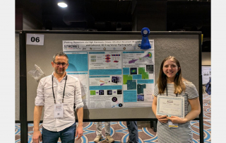
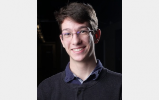
masonlw

Home \ Lauren Mason

About Lauren Mason

This author has not yet filled in any details.
So far Lauren Mason has created 320 blog entries.

An ultrafast microscope makes movies one femtosecond at a time

New CU Boulder research harnesses the power of an ultrafast microscope to study molecular movement in space and time.

The interactions in photovoltaic materials that convert light into electricity happens in femtoseconds. How fast is that? One femtosecond is a quadrillionth of a second­­. To put that in perspective, the difference between a second and a femtosecond is comparable to the difference between the second right now and 32 million years ago.

Subatomic particles like electrons move within atoms, and atoms move within molecules, in femtoseconds. This speed has long presented challenges for researchers working to make more efficient, cost-effective and sustainable photovoltaic materials, including solar cells. Imaging materials on the nanoscale with high enough spatial resolution to uncover the fundamental physical processes poses an additional challenge.

Understanding how, where and when electrons move, and how their movement depends on the molecular structure of these materials, is key to honing them or developing better ones.

Ultrafast nano-imaging of structure and dynamics in a perovskite quantum material also used for photovoltaic applications. Different femtosecond laser pulses are used to excite and measure the material. They are focused to the nanoscale with an ultrasharp metallic tip. The photo-excited electrons and coupled changes of the lattice structure (so called polarons, red ellipses) are diagnosed spectroscopically with simultaneous ultrahigh spatial and temporal resolution. (Illustration: Branden Esses)

Building on more than five years of research developing a unique ultrafast microscope that can make real-time “movies” of electron and molecular motion in materials, a team of University of Colorado Boulder scientists published in Science Advances the results of significant innovations in ultrafast nanoimaging, visualizing matter at its elementary atomic and molecular level.

The research team, led by Markus Raschke, professor of physics and JILA fellow, applied the ultrafast nanoimaging techniques they developed to novel perovskite materials. Perovskites are a family of organic-inorganic hybrid materials that are efficient at converting light to electricity, generally stable and relatively easy to make…

Revolutionizing microscopy: 25 years of computational imaging breakthroughs

UCLA physicist John Miao pioneered a new form of microscopy with unprecedented precision and field of view.  In 1999, then-graduate student Jianwei “John” Miao and his colleagues at the State University of New York, Stony Brook, demonstrated that a computational algorithm, combined with patterns of scattered photons, could reveal miniscule details previously impossible to capture with conventional microscopes.

Building on an established method for determining atomic structures called X-ray crystallography, they expanded its application to structures that lack the uniform, repeating patterns found in crystals. The algorithm reconstructs images from diffraction patterns — the arrangement of electromagnetic beams after they are bent and scattered as they pass through samples. This technique diverges from traditional microscopy by combining diffraction and computation to effectively replace the objective lens.

If you imagine microscopes as computer hardware, Miao’s approach is the “killer app” that unlocks their full potential. Over the past 25 years, scientists have integrated this approach into different types of microscopes, driving the field of computational microscopy to achieve unparalleled resolution and precision, and to capture the broadest fields of view yet on samples under investigation. These advances have led to brand-new insights into the structure and behavior of catalysts, superconductors, computer chips and next-generation batteries and materials…

Congratulations to Iona Binnie for Receiving Best Poster Award at the MMM-Intermag Conference 2025

Graduate Student Iona Binnie has received the Best Poster Award for her poster titled “Enhanced High Harmonic Generation Beamline for Ultrafast Resonant Magnetic Scattering” at the 2025 Joint MMM-Intermag Conference in New Orleans. Congratulations, Iona!

Congratulations to Franklin Dollar for Receiving the Presidential Early Career Award for Scientists and Engineers (PECASE)

Today, President Biden awarded nearly 400 scientists and engineers the Presidential Early Career Award for Scientists and Engineers (PECASE), the highest honor bestowed by the U.S. government on outstanding scientists and engineers early in their careers.

Established by President Clinton in 1996, PECASE recognizes scientists and engineers who show exceptional potential for leadership early in their research careers. The award recognizes innovative and far-reaching developments in science and technology, expands awareness of careers in science and engineering, recognizes the scientific missions of participating agencies, enhances connections between research and impacts on society, and highlights the importance of science and technology for our nation’s future.

From Day One of his Administration, President Biden has recognized the important role that science and technology plays in creating a better society. He made historic progress, increasing federally funded research and development and deploying past research and development at an unprecedented scale through the Bipartisan Infrastructure Law, the Inflation Reduction Act, and the CHIPS and Science Act.

This year’s awardees are employed or funded by 14 participating agencies within the Departments of Agriculture, Commerce, Defense, Education, Energy, Health and Human Services, Interior, Transportation, and Veterans Affairs and the Environmental Protection Agency, the intelligence community, the National Aeronautics and Space Administration, the National Science Foundation, and the Smithsonian Institution.

Congratulations to Clay Klein for Receiving the 2025 Nick Cobb Memorial Scholarship from SPIE

STROBE and JILA graduate student Clay Klein has been awarded the prestigious 2025 Nick Cobb Memorial Scholarship, presented by SPIE, the International Society for Optics and Photonics, and Siemens EDA. The scholarship, valued at $10,000, recognizes Klein’s outstanding contributions to the field of optics and photonics.

“I am honored to be awarded the Nick Cobb Memorial Scholarship,” Klein stated. “This scholarship provides me with the exciting opportunity to share my research in this field and connect with others in the industry at the SPIE conference in February.”

Klein conducts research in the laboratories of JILA Fellows and University of Colorado Boulder Physics professors Margaret Murnane and Henry Kapteyn. His work focuses on cutting-edge advancements in nanoscale extreme ultraviolet imaging science.

The award will be formally presented during the Welcome and Plenary Presentation at the SPIE Advanced Lithography + Patterning Conference in San Jose, California, on February 24, 2025. Congratulations Clay!

Postdoctoral Research Associate – An advanced X-ray characterization technique for angstrom era semiconductor patterning

The NSLS-II is seeking an exceptional Postdoctoral Research Associate to join a co-design research effort that aims at advancing extreme ultraviolet lithography (EUVL) nanofabrication well beyond the conventional lithography approaches, taking advantage of the world-leading expertise in X-ray metrology at NSLS-II, nanofabrication at the Center for Functional Nanomaterials (CFN), and machine learning (ML) at the Computational Science Initiative (CSI).

The selected candidate will collaborate with scientists at CFN and CSI to optimize the EUVL performance through rigorous simulations as well as machine-learning networks that account for the light-matter interactions in various wavelength regimes, and real light source parameters such as coherence, polarization, monochromaticity, and flux uniformity. The candidate is also expected to conduct x-ray characterizations at beamlines, using state-of-the-art microscopy techniques like coherent scattering and ptychographic imaging. The candidate will actively collaborate with researchers at external facilities such as the Advanced Light Source of Lawrence Berkeley National Laboratory and the X-ray Interference Lithography beamline at Paul Scherrer Institute of Swiss Light Source. As part of the Imaging & Microscopy team at NSLS-II, the candidate will have opportunities to collaborate using the state-of-the-art capabilities of the imaging and microscopy beamlines at NSLS-II.

Postdoctoral Appointee – Microelectronics characterization

The Instrumentation Division seeks an exceptional Postdoctoral Research Associate to join a research effort on characterization of advanced microelectronic structures using ptychographic imaging techniques being developed at NSLS-II. The x-ray metrology pipeline will be utilized for characterization of microelectronic structures being developed at IO and performing x-ray measurements at NSLS-II. Examples of target areas include (but are not limited to): (i) characterization of defects due to electromigration effects in high-current density interconnects, (ii) characterization of mechanical stress and radiation-damage effects in photonics components integrated on a conventional silicon substrate and (iii) preparation of samples to be used for x-ray experiments at NSLS-II. The selected candidate will work with a team of scientists from NSLS-II, CFN (Centers for Functional Nanomaterials), CSI (Computational Science Initiative), and IO (Instrumentation Division), plus other postdoctoral researchers who are working on different aspects of the project (i.e., development of ptychographic imaging techniques, performing simulations and experiments that incorporate latest machine-learning algorithms). Furthermore, the successful candidate will collaborate broadly with the other members of IO and CFN, leveraging their expertise in design and fabrication of microelectronics.

This is a 2 year appointment.

Optical Research Scientist (BS/MS level)

This position will provide support to the US Naval Research Laboratory’s Optical Materials and Devices Branch (Code 5620). Code 5620 conducts a broad range of research and development activities. This position will support activities within the branch including but not limited to:

  • Maintenance of thin film deposition and characterization systems
  • Thin film growth, processing, and characterization
  • Design and construction of laboratory experimental setups
  • Performance of a variety of research activities to assist government personnel
  • Purchasing laboratory supplies
  • Periodic presentation and reporting of research results

Minimum qualifications:

  • S. in Materials Engineering/Optics/Physics or a related discipline
  • Familiarity with thin film deposition and characterization techniques
  • Familiarity with programming languages and an ability to write laboratory control software
  • Familiarity with optics and optical systems
  • Excellent written communication skills

The preferred candidate will have:

  • An advanced degree in the above or related disciplines or equivalent work experience
  • A documented track record in publishing and presenting research results
  • Experience in growth, processing, and characterization of thin film materials
  • Experience in modeling and simulation of optical systems and devices
  • Experience working with lasers and optical system design and assembly

For more details, please contact Jason Myers (jason.d.myers21.civ@us.navy.mil).

Research Scientist in Optical Sciences

Summary: NRL is seeking a Research Scientist to work in the U.S. Naval Research Laboratory’s Optical Materials and Devices Branch (Code 5620) within the Optical Sciences Division. Code 5620 conducts fundamental and applied research on a broad range of optical materials, photonic devices, and systems. Responsibilities include but are not limited to:

  • Modeling and design of devices including metamaterials, integrated optic waveguides, and random or periodic nanostructures
  • Lithographic patterning of standard and non-standard materials
  • Material and device characterization including microscopy, ellipsometry, and spectroscopy
  • Preparing publications and presentations to report research results
  • Development and writing of research proposals
  • Development of relationships with research sponsors and other scientists outside of NRL
  • Willingness to assist and support other researchers on a variety of programs to meet objectives

Minimum qualifications:

  • S. citizen with an ability to obtain and maintain a security clearance
  • S. or a higher degree in Optics, Materials Science, Materials Engineering, Physics, Electrical Engineering or a related discipline
  • Expertise in modeling photonic devices
  • Laboratory skills including lithography and material and device characterization
  • Familiarity with programming languages and an ability to write laboratory control software
  • Familiarity with optics and optical systems
  • Familiarity with characterization techniques such as electron microscopy, ellipsometry, spectroscopy, and optical microscopy
  • Excellent written communication skills

Preferred qualifications:

  • D. degree in Optics, Materials Science, Materials Engineering, Physics, Electrical Engineering or a related discipline
  • Experience modeling and/or fabricating subwavelength antireflective surface structures in optics
  • Experience with deposition of thin films of optical materials
  • Familiarity with MATLAB, COMSOL, and Lumerical

For more details, please contact Jason Myers (jason.d.myers21.civ@us.navy.mil).

Go to Top