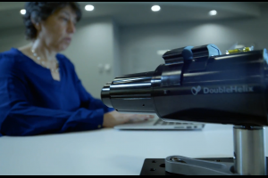
Stroboscopic Imaging of Nanoscale Transport
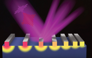
The functional properties of photovoltaics and nano-devices for electronics, thermoelectrics and data storage can be enhanced by tuning their structure at the nanoscale. However, at dimensions <100nm, bulk models can no longer accurately predict heat, charge or spin transport, or the mechanical properties of doped or nano-structured materials. A STROBE team from CU Boulder, UC Berkeley, and LBNL developed a real-time microscope to capture, map and understand nanoscale heat transport in nanostructures. This microscope was then used to validate a very surprising prediction—that an array of closely-spaced nanoscale heat sources can cool more quickly than when spaced far apart.
