UCLA scientists create world’s smallest ‘refrigerator’
How do you keep the world’s tiniest soda cold? UCLA scientists may have the answer.
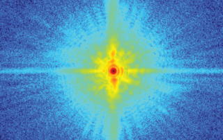
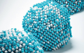
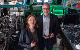
A team led by UCLA physics professor Chris Regan has succeeded in creating thermoelectric coolers that are only 100 nanometers thick — roughly one ten-millionth of a meter — and have developed an innovative new technique for measuring their cooling performance.
“We have made the world’s smallest refrigerator,” said Regan, the lead author of a paper on the research published recently in the journal ACS Nano.
To be clear, these miniscule devices aren’t refrigerators in the everyday sense — there are no doors or crisper drawers. But at larger scales, the same technology is used to cool computers and other electronic devices, to regulate temperature in fiber-optic networks, and to reduce image “noise” in high-end telescopes and digital cameras.