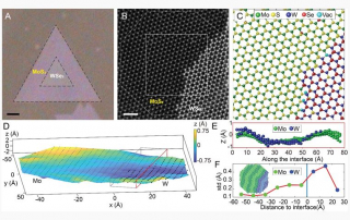
Nano-imaging functional materials at their elementary scale
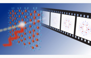
Any realistic operation of quantum technologies will require counteracting the effects of dissipation and dephasing. In particular, the wide range of photovoltaic, molecular electronic, or novel semiconductors are subject to many coupled internal degrees of freedom, structural heterogeneities, and coupling to the environment leading to the premature loss from conduction carriers to quantum information. Understanding and ultimately controlling the coupled quantum dynamics requires imaging the elementary excitations on their natural time and length scales. To achieve this goal, STROBE developed a new scanning probe microscope with ultrafast and shaped laser pulse excitation for multiscale spatial, spectral, and temporal optical nano-imaging. In this work the researchers developed heterodyne visible-pump IR-probe nano-imaging with far from equilibrium excitation to selectively probe excited state dynamics related to material function. In corresponding ultrafast movies, the fundamental quantum dynamics down to the few-femtosecond regime with nanometer spatial resolution can be resolved. This allowed to visualize in space and time competing electron and phononic processes in the application to solar-cell relevant polaron dynamics in perovskites as well as the insulator-to-metal transition in a correlated quantum material. Resolving these elementary processes related to the performance of these and other functional materials provides a perspective for the future targeted design of optimized and novel photonic and electronic material systems.