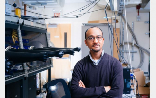
masonlw

Home \ Lauren Mason

About Lauren Mason

This author has not yet filled in any details.
So far Lauren Mason has created 240 blog entries.

Simultaneous Successive Twinning Captured by Atomic Electron Tomography

Shape-controlled synthesis of multiply twinned nanostructures is an important area of study in nanoscience, motivated by
the desire to control the size, shape, and terminating facets of metal
nanoparticles for applications in catalysis and other technologies. Controlling both the size
and shape of solution-grown nanoparticles relies on an understanding
of how synthetic parameters alter nanoparticle structures during
synthesis. However, while nanoparticle populations at the end of synthesis can be studied with standard electron microscopy methods, transient
structures that appear during some synthetic routes are difficult to observe. This is because these structures are often polycrystalline, with complicated overlapping crystal grains when that are difficult to interpret from a two-dimensional image.

A STROBE team from UC Berkeley and LBNL collaborated to study the
prevalence of transient structures during growth of multiply twinned
particles while also employing atomic electron tomography to reveal the atomic-scale three-dimensional structure of a Pd nanoparticle undergoing a shape transition, from decahedron to icosahedron. By identifying over 20,000 atoms within the structure, then classifying them according to their local crystallographic environment, we observe a multiply twinned structure consistent with a simultaneous successive twinning from a decahedral to icosahedral structure.

Imaging the electron wind force

Electromigration is one of the most critical problems limiting the future scaling of integrated circuits (ICs).  As more transistors are packed into ever smaller volumes, the total length of interconnecting wire is increasing as the wire simultaneously becomes narrower and more vulnerable to failure. Surprisingly, while chip fabs are presently churning out microprocessors at the “5-nm process node” with correspondingly tiny interconnects, before recent work by a STROBE team no measurements of electromigration pressures had been reported at length scales smaller than 10 μm.

Using electron-beam lithography, the  team fabricates tiny aluminum nanowires on electron-transparent silicon nitride membranes. They then apply an electrical current density of 108 A/cm2,  which is enough to drive electromigration, and map the nanowire’s density with parts-per-thousand precision using electron energy loss spectroscopy (EELS) in a scanning transmission electron microscope (STEM).  Two separable effects appear.  First, thermal expansion decreases the wire’s density as Joule heating raises its temperature. Using aluminum’s known coefficient of thermal expansion, one can convert the density map into a temperature map with the same spatial resolution.  Second, via the electron “wind force” the electrical current simultaneously compresses one end of the wire while it tensions the other. Using aluminum’s known bulk modulus,  one can convert the density map into a pressure map.  The temperature effect is independent of the direction of the current, while the pressure effect changes sign with the current’s direction, which allows the two effects to be separated.  Thus the thermodynamic state variables T and P can be mapped with high spatial resolution everywhere inside the wire. The ability to simultaneously see the prompt thermal and electron-wind-force effects in nanoscale interconnects opens entirely new avenues for studying electromigration, a key technological problem in the microprocessors powering modern computing devices.

Nano-imaging functional materials at their elementary scale

Any realistic operation of quantum technologies will require counteracting the effects of dissipation and dephasing. In particular, the wide range of photovoltaic, molecular electronic, or novel semiconductors are subject to many coupled internal degrees of freedom, structural heterogeneities, and coupling to the environment leading to the premature loss from conduction carriers to quantum information. Understanding and ultimately controlling the coupled quantum dynamics requires imaging the elementary excitations on their natural time and length scales. To achieve this goal, STROBE developed a new scanning probe microscope with ultrafast and shaped laser pulse excitation for multiscale spatial, spectral, and temporal optical nano-imaging. In this work the researchers developed heterodyne visible-pump IR-probe nano-imaging with far from equilibrium excitation to selectively probe excited state dynamics related to material function. In corresponding ultrafast movies, the fundamental quantum dynamics down to the few-femtosecond regime with nanometer spatial resolution can be resolved. This allowed to visualize in space and time competing electron and phononic processes in the application to solar-cell relevant polaron dynamics in perovskites as well as the insulator-to-metal transition in a correlated quantum material. Resolving these elementary processes related to the performance of these and other functional materials provides a perspective for the future targeted design of optimized and novel photonic and electronic material systems.

Unveiling the spontaneous blistering of graphene

The outstanding electrical and optical properties of graphene are intricately linked to its extraordinary mechanical behaviors. We report that for monolayer and few-layer graphene on common silicon and glass substrates, acidic solutions induce fast, spontaneous generation of solution-enclosing blisters/bubbles. Using interference reflection microscopy (IRM), a method we developed to visualize graphene structure and defects with outstanding contrast, we monitor the blister-generating process in situ, and show that at pH<~2, nanoscale to micrometer-sized graphene blisters, up to ~100 nm in height, are universally generated with high surface coverages on hydrophilic, but not hydrophobic, surfaces. The spontaneously generated blisters are highly dynamic, with growth, merging, and reconfiguration occurring at second-to-minute time scales. Moreover, we show that in this dynamic system, graphene behaves as a semipermeable membrane that allows the relatively free passing of water, impeded passing of the NaCl solute, and no passing of large dye molecules. Consequently, the blister volumes can be fast and reversibly modulated by the solution osmotic pressure.

Assessing student engagement with teamwork in an online, large-enrollment course-based undergraduate research experience in physics

Over the last decade, course-based undergraduate research experiences (CUREs) have been recognized as a way to improve undergraduate science, technology, engineering, and mathematics education by engaging students in authentic research practices. One of these authentic practices is participating in teamwork and collaboration, which is increasingly considered to be an important component of undergraduate research experiences and laboratory classes. For example, the American Association of Physics Teachers Recommendations for the Undergraduate Physics Laboratory Curriculum suggest that one of the goals for students in physics labs should be to develop “interpersonal communication skills” through “teamwork and collaboration.” Teamwork can have tremendous benefits for students, including increased motivation, creativity, and reflection; however, it can also pose an array of new social and environmental challenges, such as differing styles of communication, levels of commitment, and understanding of concepts. It can also be difficult for lab course instructors to evaluate and assess. In this work, we study student teamwork in a large-enrollment physics CURE. The CURE was specifically designed to emphasize teamwork as a scientific practice. We use the two sources of data, the adaptive instrument for regulation of emotions questionnaire and students’ written memos to future researchers, to measure the students’ teamwork goals, challenges, self, co-, and socially shared regulations, and perceived goal attainment. We find that students overwhelmingly achieved their teamwork goals by overcoming obstacles using primarily socially shared regulatory strategies, and that the vast majority of students felt teamwork was an essential part of their research experience. We discuss implications for the design of future CUREs and lab courses and for lab instructors desiring to assess teamwork in their own courses.

Structural and Elastic Properties of Nanostructured Materials Extracted Via Nondestructive Coherent Extreme UV Scatterometry and Electron Tomography

Semiconductor metalattices consisting of a linked network of 3D nanostructures with periodicities on length scales <100nm can enable tailored functional properties due to their complex nanostructuring. For example, by controlling both the porosity and pore size, thermal transport in these phononic metalattices can be tuned—making them promising candidates for efficient thermoelectrics or thermal rectifiers. Thus, the ability to characterize the porosity, and other physical properties, of metalattices is critical but challenging, due to their nanoscale structure and thickness. To date, only metalattices with high porosities, close to the close-packing fraction of hard spheres, have been studied experimentally. Recently, a STROBE team characterized the porosity, thickness, and elastic properties of a low-porosity, empty-pore silicon metalattices for the first time. Laser-driven nanoscale surface acoustic waves were probed by EUV scatterometry to nondestructively measure the acoustic dispersion in these thin silicon metalattice layers. The Young’s modulus, porosity and metalattice layer thickness were then extracted. These advanced characterization techniques are critical for informed and iterative fabrication of energy-efficient devices based on nanostructured metamaterials.

Capturing 3D atomic defects and phonon localization at the 2D heterostructure interface

2D lateral and vertical heterostructures have been actively studied for fundamental interest and practical applications. Although aberration-corrected electron microscopy and scanning probe microscopy have been used to characterize a wide range of 2D heterostructures, the 3D local atomic structure and crystal defects at the heterostructure interface have thus far defied any direct experimental determination. Now, a collaborative team from UCLA, Harvard University, MIT and UC Irvine demonstrates a correlative experimental and first principles method to determine the 3D atomic positions and crystal defects in a MoS2-WSe2 heterojunction with picometer prevision and capture the localized vibrational properties at the epitaxial interface. They observe various crystal defects, including vacancies, substitutional defects, bond distortion and atomic-scale ripples, and quantitatively characterize the 3D atomic displacements and full strain tensor across the heterointerface. The experimentally measured 3D atomic coordinates, representing a metastable state of the  heterojunction, are used as direct input to first principles calculations to reveal new phonon modes localized at the heterointerface, which are corroborated by spatially resolved electron energy-loss spectroscopy. In contrast, the phonon dispersion derived from the minimum energy state of the  heterojunction is absent of the local interface phonon modes, indicating the importance of using experimental 3D atomic coordinates as direct input to better predict the properties of heterointerfaces. Looking forward, it is expected that the ability to couple the 3D atomic structures and crystal defects with the properties of heterostructure interfaces will transform materials design and engineering across different disciplines.

Revealing trimer cluster superstructures at ultrafast timescales in TaTe2

Understanding and controlling the forces that drive the formation of symmetry-broken phases in quantum materials is a key challenge in condensed matter physics. The nature of the correlated interplay between charge, spin, and lattice degrees of freedom, however, often remains hidden in equilibrium studies where adiabatic tuning masks the causal ordering of rapid interactions. This motivates the use of ultrafast electron diffraction (UED) to capture structural dynamics on intrinsic time scales, for insight into the role of atomic-scale lattice distortions and vibrational excitations in driving, stabilizing and ultimately controlling emergent phases.

In a recent publication, a STROBE team carried out the first-ever ultrafast study of tantalum telluride (TaTe2), yielding direct insight into its structural dynamics. The material exhibits unique periodic charge and lattice trimer order, which transitions from stripe-like chains into a (3×3) superstructure of trimer clusters at low temperatures. After cooling to 10 K, the thin crystalline films were optically excited and the structural dynamics was probed with the high-brightness electron bunches. Satellite peaks as well as sign changes in the complex diffraction patterns yield a fingerprint of the periodic order and structural transition. Our experiments captured the photo-induced melting of the trimer clusters in TaTe2, evidencing an ultrafast phase transition into the stripe-like phase on a ~1.4 ps time scale. Subsequently, thermalization into a hot cluster superstructure occurred. Density-functional calculations indicate that the initial quench is triggered by intra-trimer Ta charge transfer, which destabilizes the clusters unlike CDW melting in other TaX2 compounds.

Critical to this project were new methods and algorithms, enhanced microscopes and samples, advanced sample preparation as well as a unique high repetition rate ultrafast electron diffraction beamline utilized by the STROBE team from UC Berkeley, LBNL and UCLA

Congratulations to Margaret Murnane for Being Named One of the Best Female Scientists in the World in 2022

Margaret Murnane is one of five women scientists in Colorado named among the best in the world. The 1st edition of Research.com ranking of top female scientists in the world is based on data collected from Microsoft Academic Graph on 06-12-2021. Position in the ranking is based on a scientist’s general H-index. The Research.com ranking of top female scientists in the world includes leading female scientists from all major areas of science. It was based on a meticulous examination of 166,880 scientists on Google Scholar and Microsoft Academic Graph.

Congratulations to Jose Rodriguez for Receiving Tenure at UCLA

Professor Jose Rodriguez received tenure at UCLA in the Department of Chemistry and Biochemistry. Congratulations, Jose!

Prof. Jose Rodriguez received his Ph. D in Molecular Biology from UCLA in 2012. He was then a Postdoctoral Researcher at UCLA and subsequently joined the Department of Chemistry & Biochemistry as assistant professor in 2016.

Go to Top