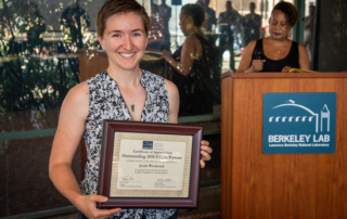
News

Home \ News

Congrats to Chris Regan and William Hubbard for Receiving the 2019 Microscopy Today Innovation Award

The editors of Microscopy Today congratulate the winners of the tenth Microscopy Today Innovation Award competition. The ten innovations advance microscopy in several areas: light microscopy, electron microscopy, and scanning probe microscopy. These innovations will make microscopy and microanalysis more powerful, more productive, and easier to accomplish.Secondary Electron Electron-BeamInduced-Current (SEEBIC) Imaging University of California at Los Angeles Developers: Chris Regan and William Hubbard. While intimately related to prior electron-beaminduced-current (EBIC) methods in the SEM, secondary electron electron-beaminduced-current (SEEBIC) imaging is qualitatively and quantitatively different. What makes the SEEBIC system new is that both the secondary electron (SE) and hole signals are detected in a scanning transmission electron microscope (STEM). SEEBIC differs from traditional EBIC in several ways. The measuring circuits are wired differently. In the former case the end of the device remote from the transimpedance amplifier is extremely high impedance, while in the latter it is tied to a low impedance (usually ground) to allow charge neutralization. While traditional EBIC imaging is sensitive to holes, it only generates contrast in regions where the sample supports an electric field that will separate electron-hole pairs. In most samples such regions are special and localized, for example, in a p-n junction. Thus, most of the sample generates no contrast when imaged with traditional EBIC. SEEBIC, on the other hand, is an inevitable consequence of imaging a thin specimen with an energetic electron beam, and SEEBIC imaging generates contrast everywhere in a sample. SEEBIC imaging has not been demonstrated previously for a couple reasons. First, the typical SEM sample is electron-opaque, and primary beam absorption produces a large background; thus, the SEEBIC signal is buried in the noise of the traditional SEM EBIC apparatus. This background is largely absent in the electron-transparent samples used in STEM. Secondly, the secondary electron (SE) yield drops with increasing beam energy; therefore, the SE signal is even smaller in a 200 kV STEM than in a 30 kV SEM. Detection of the signal requires a current measuring system that is low-noise and protected from electromagnetic interference (1 pA EBIC corresponds to ∼6,000 electrons in a 1 ms dwell time). SEEBIC is sensitive to electric potential, electric field, work function, conductivity, and temperature, and it can probe these quantities with atomic resolution in a modern STEM. STEM SEEBIC can image a functioning resistive random access memory (RRAM). For example, in a HfO2-based RRAM, the conducting filament is thought to consist of oxygen vacancies. Oxygen vacancies are basically invisible in a standard STEM image, but they give excellent contrast when viewed with STEM EBIC imaging.

KMLabs QM Quantum Microscope an R&D 100 Awards winner

Winners of the R&D 100 Awards have been announced by R&D World magazine and its new parent company, WTWH Media, LLC.

We are proud to announce that the QM Quantum Microscope™ is one of this year’s winners.  The QM Quantum Microscope builds on the company’s world leading technology in high harmonic generation to enable a range of techniques including coherent diffraction imaging, photoemission, pump-probe spectroscopy, and EUV metrology.

Primary Contributors to the project include:

JILA: Michael Tanksalvala, Yuka Esashi, Christina Porter, Michael Gerrity, Ting Liao, Margaret Murnane

KMLabs: Seth Cousin, Daisy Raymondson, Brennan Peterson, Henry Kapteyn

“Microscopes illuminated by coherent extreme UV beams are extremely sensitive to structure, composition and function at the nanoscale. They represent an entirely new class of lab scale microscope, with unique capabilities that are critical for future semiconductor, energy, solid state chemistry, and quantum devices.’ Henry Kapteyn, CTO.

About KMLabs: KMLabs is the only commercial provider for comprehensive, end-to-end research systems that leverage ultrafast pulses of extreme UV and soft X-ray light for a variety of experiments. The QM Quantum Microscope™ builds on the company’s world leading technology in high harmonic generation to enable a range of techniques including coherent diffraction imaging, photoemission, pump-probe spectroscopy, and EUV metrology. In addition, KMLabs continues to pioneer the development and engineering of standalone short wavelength sources including the Y-Fi VUV laboratory-based vacuum ultraviolet femtosecond laser source, and the Pantheon™ platform, a pulsed EUV source-beamline to generate and deliver EUV photons to user-supplied experimental stations.

2019 R&D 100 Award winners unveiled!

Winners of the R&D 100 Awards have been announced by R&D World magazine and its new parent company, WTWH Media, LLC. “This awards program is so well recognized across the R&D community. Being named as one of the R&D 100 is an incredible honor,” said Paul J. Heney, Vice President, Editorial Director for R&D World. “These 100 winning products and technologies are the disruptors that will change industries and make the world a better place in the coming years.”

Analytical/Test Category:

QM Quantum Microscope – Next Generation Microscopy & Analysis
KMLabs, Inc.
JILA at the University of Colorado, the STROBE center

Congrats to Michael Tanksalvala, Yuka Esashi, Christina Porter, Michael Gerrity, Ting Liao, Margaret Murnane (JILA), Seth Cousin, Daisy Raymondson, Brennan Peterson, and Henry Kapteyn (KMLabs) for Receiving the R&D 100 Award for the QM Quantum Microscope

Winners of the R&D 100 Awards have been announced by R&D World magazine and its new parent company, WTWH Media, LLC. “This awards program is so well recognized across the R&D community. Being named as one of the R&D 100 is an incredible honor,” said Paul J. Heney, Vice President, Editorial Director for R&D World. “These 100 winning products and technologies are the disruptors that will change industries and make the world a better place in the coming years.”

Analytical/Test Category:

QM Quantum Microscope – Next Generation Microscopy & Analysis
KMLabs, Inc.
JILA at the University of Colorado, the STROBE center

Real-time imaging for use in medicine

A new paper in Nature Photonics from researchers at CU Boulder details impressive improvements in the ability to control the propagation and interaction of light in complex media such as tissue—an area with many potential applications in the medical field. Published Monday, the paper is titled “Wavefront shaping in complex media with a 350 kHz modulator via a 1D-to-2-D transform.” The work was carried out in Professor Rafael Piestun’s lab in the Electrical, Energy and Computing Engineering Department. The team included CU Boulder post-doctoral researchers Omer Tzang and Simon Labouesse, researcher Eyal Niv and CU Boulder graduate student Sakshi Singh. Greg Myatt from Silicon Light Machines, a collaborating company in this project, also worked with the group.

Congrats to Jessie Woodcock for Receiving an Outstanding 2018 STEM Partner Award in recognition of partnership and support of Workforce Development & Education programs

On Thursday, September 26, Workforce Development & Education hosted our annual Mentor Appreciation event where we recognized our outstanding mentors and STEM partners. This event highlighted accomplishments for FY2018. Outstanding 2018 STEM Partner is hereby awarded on this 26th day of September 2019, to Jessie Woodcock, in recognition of partnership and support of Workforce Development & Education programs.

Congratulations to Josh Knobloch for receiving a 2019 TECHCON Student Presentation Award

Thank you to the SRC students, industry, and faculty that attended TECHCON and made it a great success. The final event for TECHCON 2019 was presenting Top 10 Student Presentation Awards and the URI Best Poster Awards at Tuesday’s Dinner.

2019 TECHCON Student Presentation Award Winner:

Joshua Knobloch
Nanoscale Metrology and Imaging of Layered and Nano-enhanced Materials using Coherent Extreme Ultraviolet Beams

Watching crystal nucleation happen at atomic scale

Crystals form in storm clouds, metals, drug molecules, and even in diseased tissues. Despite their ubiquity, scientists still don’t fully understand what happens when a liquid solution first starts to form a solid crystal, a step called nucleation. Now researchers have gotten their first glimpse of the details of the process, imaging individual atoms during nucleation in metal nanoparticles (Nature 2019, DOI: 10.1038/s41586-019-1317-x).

First 4D look at crystallising atoms contradicts textbook nucleation theory

For the first time scientists have watched iron and platinum atoms crystallise in 4D – not only observing their arrangement in space but tracking them over time. Their observations clash with classical nucleation theory, which describes the early stages of a phase transition, adding to growing evidence that the textbook theory is outdated and imprecise.

Atomic motion is captured in 4D for the first time

Results of UCLA-led study contradict a long-held classical theory.

Everyday transitions from one state of matter to another — such as freezing, melting or evaporation — start with a process called “nucleation,” in which tiny clusters of atoms or molecules (called “nuclei”) begin to coalesce. Nucleation plays a critical role in circumstances as diverse as the formation of clouds and the onset of neurodegenerative disease.

A UCLA-led team has gained a never-before-seen view of nucleation — capturing how the atoms rearrange at 4D atomic resolution (that is, in three dimensions of space and across time). The findings, published in the journal Nature, differ from predictions based on the classical theory of nucleation that has long appeared in textbooks.

Go to Top