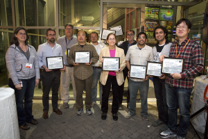
News

Home \ News

Tracking Energy Flow in Light-harvesting Systems on Native Nanometer and Picosecond Scales

So Ginsberg and her colleagues devised a measurement that transforms an optical “super-resolution” microscopy known as STED (stimulated emission depletion) into a tracker of excitons on these short scales in an organic semiconductor. The technique makes it possible, for the first time, to relate the characteristics of exciton migration efficiency to nanoscale structures within light harvesting materials. “We ended up using the spatial profile of light pulses and the way that they interact with the material in order to excite very small and localized regions that have very sharp boundaries,” she said.

APS TV Features STROBE at JILA

STROBE is featured in an APS TV video about what makes JILA a unique and great place to work. JILA is a unique research and training partnership between the University of Colorado and the National Institute of Standards & Technology. At JILA, scientists develop new research and measurement technologies that broadly advance science and the NIST measurement mission. To date, JILA scientists have been awarded three Physics Nobel Prizes. JILA also trains young innovators who become leaders in industry, academia, and government labs. And after traveling to the many laboratories housed at JILA, APS TV discovers that collaboration amongst its researchers is one of its greatest strengths.

Congrats to Robert Karl Jr. on Receiving the Karel Urbanek Student Paper Award at SPIE Advanced Lithography 2018

We are happy to share the 2018 winner of the Karel Urbanek Student Paper Award at #SPIELitho, Robert Karl Jr., from JILA! His paper was entitled, “Characterization and Imaging of Nanostructured Materials using Tabletop Extreme Ultraviolet Light Sources”. KLA-Tencor is honored to be the sponsor of this annual award at this year’s Metrology, Inspection, and Process Control for Microlithography conference at SPIE Advanced Lithography 2018 in San Jose, California.

Congrats to Jose Rodriguez on Being Selected as a Beckman Young Investigator by the Arnold and Mabel Beckman Foundation

Professor Jose Rodriguez has been selected as a Beckman Young Investigator by the Arnold and Mabel Beckman Foundation… According to the Beckman Foundation website, “these individuals exemplify the Foundation’s mission of supporting the most promising young faculty members in the early stages of their academic careers in the chemical and life sciences, particularly to foster the invention of methods, instruments and materials that will open new avenues of research in science. They were selected from a pool of over 300 applicants after a three-part review led by a panel of scientific experts.”

Congrats to Stan Osher on being elected as a member of the National Academy of Engineering

Election to the National Academy of Engineering is among the highest professional distinctions accorded to an engineer.  Academy membership honors those who have made outstanding contributions to “engineering research, practice, or education, including, where appropriate, significant contributions to the engineering literature” and to “the pioneering of new and developing fields of technology, making major advancements in traditional fields of engineering, or developing/implementing innovative approaches to engineering education.”

Congrats to Jianwei “John” Miao on Receiving the NSF Special Creativity Award

A rarely given Special Creativity Award from the National Science Foundation has been recently bestowed to a pair of UCLA faculty members, along with a leading computer simulation expert at the University of Colorado Boulder, to continue their research on metal alloys for fuel cells.

The principal investigators on the grant are Jianwei “John” Miao, UCLA professor of physics and astronomy and also the deputy director, NSF STROBE Science and Technology Center; Yu Huang, UCLA professor of materials science and engineering; and Hendrik Heinz, an associate professor of chemical and biological engineering at the University of Colorado Boulder.  Huang and Miao are also members of the California NanoSystems Institute at UCLA.

Photo Credit: Reed Hutchinson/UCLA

Berkeley Lab’s Molecular Foundry (MF) hosted the Frontiers of Electron Tomography in the Physical Sciences

Berkeley Lab’s Molecular Foundry (MF) hosted the Frontiers of Electron Tomography in the Physical Sciences conference together with UCLA and STROBE (an NSF Science and Technology Center) to disseminate results and discuss new ideas for three-dimensional imaging techniques.  The conference was held in Berkeley, CA from October 23rd – 26th and included a two-day workshop of research talks followed by a two-day short course. A total of 97 people registered for the conference.

Tomography is a technique that can reconstruct the three-dimensional shape of objects at the nanoscale from a series of two-dimensional images such as those acquired by scanning / transmission electron microscopy (S/TEM). It has become an increasingly important technique in nanoscale research for quantitative characterization in three-dimensions of a wide range of materials systems. Recent advances in S/TEM hardware and reconstruction algorithms has extended this technique to the atomic scale in a technique known as atomic electron tomography (AET). A joint collaboration between UCLA and the MF, with funding from DOE BES and STROBE, has proven atomic resolution imaging is possible with precision of 19 trillionths of a meter (19 picometers). The FET2017 conference was held to discuss these new capabilities, potential future applications and provide in-depth teaching of the technique to graduate and postdoctoral students.

The two-day workshop included talks by several internationally recognized speakers on electron imaging and tomography as well as a poster session highlighting student research. Attendees were given the opportunity to take part in discussions on improvements and applications to AET. An important discussion during the workshop focused on the need for a materials data bank (MDB) of atomic resolution data sets and experimentally determined atomic coordinates made available openly to the physical sciences research community. This database, currently under development, will provide peer-reviewed sets of atomic structures and should be available in 2018.

After the workshop, tomography experts taught two days of lectures and hands-on tutorials to graduate and postdoctoral students on electron tomography topics such as theory, experimental design and newly available software. The new GENFIRE algorithm and open-source software developed as part of STROBE to reconstruct the atomic structure of materials. Also presented was the open-source Tomviz tomography analysis and visualization platform developed by Kitware, Inc. All lecture materials are available at the FET2017 short course website in an effort to increase the accessibility of the AET technique.

The conference was held jointly by the MF, UCLA and STROBE with contributions from several industry partners. More information is available at the conference website.

Synopsis: Plasmon Thermometers for Silicon

Electron oscillations in silicon may be used to map, with nanometer resolution, the temperatures across a silicon device. Chris Regan of the University of California, Los Angeles, and co-workers have now developed a thermometry technique that, using a scanning transmission electron microscope (STEM), could eventually map temperature in a silicon device with a resolution down to 10 nm.

Go to Top